Henini M. Handbook of Self Assembled Semiconductor Nanostructures for Novel devices in Photonics and Electronics
Подождите немного. Документ загружается.

InAs Quantum Dot Formation Studied at the Atomic Scale 169
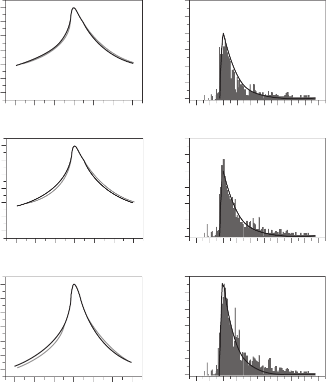
of the surface of a cleaved InAs/GaAs QD and WL as a function of the position of the cleavage
plane. The dots are considered to be truncated pyramids. The corresponding expected size distri-
bution is shown by the solid line in the graph, in which the results of a real X-STM measurement
are also shown (squares). Only after scanning a large number of cleaved dots can the maximum
base length of the cross-section of the dot be determined, which is indicative for a cleavage near
the dot centre. Only the outward relaxation profi le of the dots cleaved close to the centre (dots in
the region (d)) are used to compare with the model.
5.1.2.2 Experimental set-up
5.1.2.2.1 Sample and tip preparation
Small rectangular pieces (about 3.5 1 0 m m
2
) are cleaved from a wafer containing the semi-
conductor heterostructure of interest. These wafers are normally 350–550 μ m thick and are
polished down with aluminum oxide powder to a thickness of about 100 μm, for easy cleavage.
For an STM measurement it is essential to have good electric contact with the sample. Therefore,
metallic contacts are evaporated at the top surface of the sample after treating it with an N2/
H2 plasma. A small scratch of about 0.5–1.5 mm, which extends to a small notch at the side
of the sample, is made at the top surface of the sample using a diamond pen. This scratch facili-
tates the cleavage of the sample and provides a fi xed starting point for the propagation of the
cleavage plane. The sample is clamped on a sample holder between two metal bars that can be
screwed together, as shown in Fig. 5.6 . Only one corner of the sample is clamped for the uncon-
strained propagation of the cleavage plane. Between the metal bars and the two surfaces of the
sample, at the position where the sample is to be clamped, thin slices of indium are placed. The
sample holder is heated in order to melt the indium before tightening the screws. The indium
provides an even pressure distribution on the sample, preventing it from cleaving during tighten-
ing of the screws and slipping out of the holder when the sample is degassed subsequently in the
UHV system. The sample is cleaved in the STM chamber using a gentle touch by a manipulator
(the so-called “ wobble stick ” ) just before the measurement as shown in Fig. 5.6 . A characteristic
crack pattern is also shown in Fig. 5.6 [25]. After cleavage, the sample is placed into the sample
stage and moved towards a mounted tip, with the help of a CCD camera equipped with a tele-
lens. First, the sample is brought close to the tip and then further approached until tunnelling
contact is done automatically by the system. After the fi rst tunnelling contact, the tip is retracted
and moved several 100 nm towards the edge of the cleavage surface where the grown layers (epi-
layers) are located. The process of making tunnelling contact and moving towards the epilayers
is repeated until the tip moves over the edge of the sample. At this point tunnelling contact is not
achieved, which indicates that the location of the epilayers is within several 100 nm.
25
20
15
10
5
0
5
10
15
20
25
25
20
15
10
5
0
5
10
15
20
25
1020304050
25
20
15
10
5
0
5
10
15
20
25
1020304050
25
20
15
10
5
0
5
10
15
20
25
1020304050
10203040
50
(a)
(c)
(b)
(d)
11 12 13 14
Base length (nm)
4.5
5.0
5.5
(a)
6.0
6.5
7.0
(b)
Height (nm)
(c)
(d)
15 16 17 18 19 20
Figure 5.5 Expected (solid line) and measured by X-STM (squares) size distribution of cleaved InAs/GaAs QDs.
The different sizes correspond to dots cleaved in different positions, as shown by the calculated outward relaxation for
different cleavage planes.
CH005-I046325.indd 169CH005-I046325.indd 169 6/27/2008 4:19:25 PM6/27/2008 4:19:25 PM
170 Handbook of Self Assembled Semiconductor Nanostructures for Novel Devices in Photonics and Electronics
The tips are made of 99.97% pure polycrystalline tungsten wire with a diameter of 0.25 mm.
A short piece of this wire ( ⬃ 5 mm) is spot welded onto an Omicron tip holder and cleaned for use
in UHV. The tips are then electrochemically etched with a 2.0 molar potassium hydroxide solu-
tion. The top 1–1.5 mm of the tip is put into the solution and a positive voltage (4–5 V) is applied
to the tip wire. A platinum–iridium (90%/10%) spiral serves as a counter-electrode. As the reac-
tion products dissolve in the etchant, they sink down along the wire, which is visible from the
local change of the diffractive index of the solution. Because of the geometry, the reaction veloc-
ity is the highest at the point where the tungsten wire penetrates the surface of the solution. This
causes necking of the wire at the surface of the etching solution, as the reaction products owing
down the tip shield the rest of the wire. Eventually, the wire will break at the neck leaving a very
sharp tip. A current limiter is used to interrupt the etching process immediately ( 1 μ s) after the
breaking of the wire. The tips are degassed after loading into the UHV system and treated with a
700 eV argon ion bombardment in order to mechanically stabilize the tip.
5.1.2.2.2 The STM unit and the UHV system
A commercially available room-temperature STM unit (Omicron STM-1 TS2) is used. The STM
set-up is very sensitive to external vibrations, as the tip–sample distance during tunnelling is
only a few angstrom. Moreover, the apparent height of the atomic corrugation visible in the STM
images is only 20 pm. Therefore, the set-up is vibration isolated with different damping systems.
The scanner unit is suspended on a set of springs and stabilized by an eddy current damping sys-
tem. The eddy current damping system consists of copper fi ns that surround the scanner and are
placed between permanent magnets when the scanner unit is in its suspended position. The STM
unit, together with the rest of the set-up, is mounted on a heavy metal tabletop. Rubber damp-
ers between this tabletop and the supporting frame fi lter out high-frequency vibrations. Low-
frequency vibrations are suppressed by four active damping elements that are mounted between
the fl oor and the frame. In this active damping system several motion detectors are present and
several actuator coils counteract the detected motion of the system. Finally, the entire set-up is
standing on a heavy concrete platform that is decoupled from the building.
A factor of critical importance in cross-sectional scanning tunnelling microscopy on III/V
semiconductors is the production of an atomically fl at cross-sectional surface that is free of
contamination/oxidation, in order to obtain an electronically unpinned surface. Therefore, clea-
vage of the samples and the subsequent measurement are performed in a home-built ultra-high
vacuum set-up ( Fig. 5.7 ). The central vacuum chamber (STM), in which the STM unit is posi-
tioned, is pumped down by an ion-getter pump (IGP) with a titanium sublimation element (TSE)
to a pressure lower than 5 1 0
1 1
torr (Varian VacIon Plus, 300 litre/sec). During X-STM
110
110
001
Coarse positioning
Cleavage induced steps
Cleaved surface
Scratch Atomically flat epilayer region
Bulk region
V
BIAS
y
x
z
Push direction
Scratch Epilayers
Figure 5.6 Schematic view of the sample cleavage process.
CH005-I046325.indd 170CH005-I046325.indd 170 6/27/2008 4:19:26 PM6/27/2008 4:19:26 PM
InAs Quantum Dot Formation Studied at the Atomic Scale 171
measurements the inner panel of the IGP/TSE can be cooled down with liquid nitrogen, which
enhances the pump speed by a factor of two. In the preparation chamber (PREP), which is separated
by a valve from the STM chamber, the tips and samples can be degassed with a baking unit and
tips can be treated with an argon ion bombardment. Two oil-free turbo-molecular pumps (Varian
V-250 and V-70), installed in series, keep the preparation chamber at a pressure of approximately
6 1 0
1 0
torr. The preparation chamber is connected to a load lock, for loading and unloading
the tips and samples without seriously affecting the pressure in the preparation and STM chamber.
The load lock is pumped with one of the turbo-molecular pumps (V-70) to a pressure of about 10
6
torr. An XDS5 dry scroll pump provides the necessary pre-vacuum of about 10
1
torr. During the
X-STM measurements all pumps are switched off to prevent vibrations, except the IGP/TSE as this
pump contains no moving parts. Two wobble sticks in the STM and preparation chamber are used
for manipulation and transportation of the tips and samples.
5.2 Formation of the wetting layer
The formation of InAs wetting layers (WLs) has attracted relatively little attention compared
to quantum dot (QD) formation [26–28] . In the simple picture of Stranski–Krastanov growth,
after the build-up of a critical amount of strain, 2D layer growth is followed by QD formation. It
has become increasingly clear, however, that such a simple picture is far from reality. Recently,
In incorporation during pseudomorphic InAs/GaAs growth and QD formation was observed by
in situ stress measurements [29] .
In this section we analyse the composition and segregation of InAs WLs by either directly
counting the indium atoms or by analysis of the outward displacement of the cleaved surface as
measured by X-STM.
As mentioned in the introduction, the measured outward relaxation profi le at high nega-
tive voltage can be compared to the calculated one to deduce the In concentration in the WL.
By modelling the indium segregation, the outward displacement of the segregated WL can be
calculated by integration of the analytical expression derived by Davies for the outward displace-
ment of a cleaved quantum well [24] . Several models for indium segregation have been proposed
(Ion gun)
PREP
Load lock
Vent inlet
Table
IGP/TSP
N2
N1
V-250
V-70
Vent inlet
Active damping system
Pressure gauge
Scroll pump
S S
S S
STM
Figure 5.7 Schematic drawing of the UHV system containing the STM and damping system.
CH005-I046325.indd 171CH005-I046325.indd 171 6/27/2008 4:19:26 PM6/27/2008 4:19:26 PM
172 Handbook of Self Assembled Semiconductor Nanostructures for Novel Devices in Photonics and Electronics
[30–33] . We use the phenomenological model of Muraki et al . [31] , which has been shown to
describe well the indium composition x ( n ) of InAs WLs [28] :
xn R
RR
n
nN
nN
n
NnN
()
,
(),
(),
0
1
1
⎧
⎨
⎪
⎪
⎪
⎩
⎪
⎪
⎪
<1
1≤ ≤
>
(5.1)
where n is the monolayer (ML) index, N is the total amount of deposited indium and R is the
indium segregation coeffi cient. N and R are determined by fi tting the calculated relaxation profi le
to the measured relaxation profi le.
The WLs were grown by molecular-beam epitaxy (MBE) on doped GaAs (100) wafers. In
sample A, three different sets of WLs were grown at 495°C by deposition of 1.5 ML, 2.0 ML and
2.5 ML of InAs, respectively, at a growth rate of 0.1 ML/s. Each layer was repeated two times, sep-
arated by a 50 nm GaAs buffer layer, also grown at 495°C. A growth interruption of 10 seconds
has been applied after the growth of each layer. No dot formation was observed for the layers
with 1.5 ML indium deposition. In sample B, two sets of WLs were grown at 480°C by deposition
of 2.0 ML of InAs at a high and a low growth rate of 0.1 ML/s and 0.01 ML/s, respectively. Each
layer was repeated two times and capped by a 20 nm GaAs layer grown at 480°C, followed by a
30 nm GaAs layer grown at 580°C. A growth interruption of 10 seconds has been applied after
the growth of each layer. In sample C, one set of InAs layers was grown in GaAs while a second
set was grown in AlAs barriers. The InAs layers were grown at 500°C by deposition of 1.9 ML
of InAs in a cycled way, i.e. with a 3 second pause after each deposition of 0.25 ML, at a growth
rate of 0.043 ML/s. The following layer sequence was used: 20 nm GaAs/1.9 ML InAs/40 nm
GaAs/1.9 ML InAs/40 nm GaAs/50 nm GaAs (doped 1 1 0
18
c m
2
)/20 nm GaAs/4 ( 2 0 n m
AlAs/1.9 ML InAs/20 nm AlAs/40 nm GaAs). To reduce interface roughness, the bottom AlAs
barriers were grown at 600°C followed by a growth interruption prior to InAs deposition.
Sample A was used to study the effect of the amount of indium deposition on the WL forma-
tion. We measured the relaxation profi les of the WLs and fi tted these with calculated relaxation
profi les, by adjusting the fi t parameters N and R . The resulting segregation profi les were verifi ed
by counting directly the number of indium atoms in the WL as a function of distance in growth
direction. For the counting procedure, we selected four high-quality images of each layer, such
as the one shown in Fig. 5.8 . The relaxation and segregation profi les are shown in Fig. 5.9 .
(a)
(b)
5nm
5nm
Figure 5.8 (a) Empty states X-STM image of a segregated 2.0 ML InAs WL. The arrow indicates the growth direc-
tion. (b) The same image treated with a high-pass Fourier fi lter. The inset shows an enlarged view of part of the image.
CH005-I046325.indd 172CH005-I046325.indd 172 6/27/2008 4:19:26 PM6/27/2008 4:19:26 PM
InAs Quantum Dot Formation Studied at the Atomic Scale 173
15
0.20
0.30
0.25
0.20
0.15
0.10
0.05
0.00
4 2 2 4 6 8 1012140
(a)
(d)
1.5 ML
N 1.60.1 R 0.86 0.03
Relaxation (nm)
Concentration
0.18
0.16
0.14
0.12
0.10
0.08
10 50
X (nm)
X (nm)
51015
15
0.20
(b)
2.0 ML
Relaxation (nm)
0.18
0.16
0.14
0.12
0.10
0.08
10 5
0
X (nm)
51015
15
0.20
(c)
2.5ML
Relaxation (nm)
0.18
0.16
0.14
0.12
0.10
0.08
10 5
0
X (nm)
51015
0.30
0.25
0.20
0.15
0.10
0.05
0.00
4 2 2 4 6 8 1012140
(e)
N 1.7 0.1 R 0.87 0.03
Concentration
X (nm)
0.30
0.25
0.20
0.15
0.10
0.05
0.00
4 2 2 4 6 8 1012140
(f)
N 2.2 0.1 R 0.85 0.03
Concentration
X (nm)
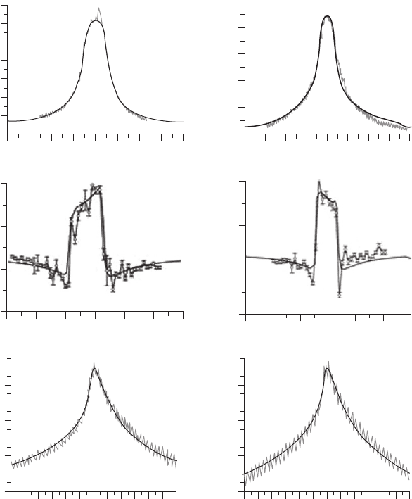
Figure 5.9 Measured and fi tted relaxation profi les of the 1.5 ML (a), 2.0 ML (b) and 2.5 ML (c) InAs WLs of
sample A. The black curves in (d), (e) and (f) show the segregation profi les corresponding to the fi tted relaxation pro-
fi les in (a), (b) and (c). The columns indicate the counted indium concentration in the WL as a function of distance X
in the growth direction.
In all three cases, we fi nd an excellent agreement between the indium profi le determined from
the outward relaxation of the surface, and the direct counting procedure. For the 1.5 ML WL, the
measured amount of indium N corresponds to the deposited amount, since no indium has gone
into dot formation. For the 2.0 ML and 2.5 ML WLs, however, we fi nd a clear indium enrichment
of the WL, despite dot formation.
In Stranski–Krastanov growth mode, strain builds up until the critical amount of indium for
dot formation is deposited [34] . It has been shown that only part of the deposited amount of
indium contributes to the strain, by incorporation into the lattice, while the remaining indium
forms a fl oating layer on the surface [29] . During dot formation, part of the fl oating indium is
transferred by lateral mass transport to the dots. The amount of indium that remains in the dots,
however, is strongly reduced by the capping process, which dissolves the top of the dots back into
the WL, as we will show in sections 5.2 and 5.4. The dissolved indium adds to the remaining
CH005-I046325.indd 173CH005-I046325.indd 173 6/27/2008 4:19:28 PM6/27/2008 4:19:28 PM
174 Handbook of Self Assembled Semiconductor Nanostructures for Novel Devices in Photonics and Electronics
fl oating indium, and is eventually incorporated into the lattice, during continued capping. That
is the reason for the observed indium enrichment of the WL after dot formation.
We used sample B to study the effect of a reduced growth rate on the WL formation. It
is known that a reduced growth rate leads to an increased QD size and a reduced QD density.
However, it is not a priori clear how this will affect the formation of the segregated WL in the
buried structure. In Fig. 5.10 we show the average measured and calculated relaxation pro-
fi les of the InAs WLs of sample B. The dashed lines indicate the relaxation profi les calculated
directly from indium atom counting using different images. We fi nd that the high (0.1 ML/s) and
low (0.01 ML/s) growth rate InAs WLs can be described by the same parameters within errors.
However, there is, as expected, a marked difference in the size of the QDs, shown in Fig. 5.11 .
Whereas the QD grown at the high growth rate appears as a rather fl at, disk-like shape with
a height of 3 nm ( Fig. 5.11a ), the QDs grown at low rate show an indium distribution with a
reversed truncated cone shape [35] with a height of 5.4 nm ( Fig. 5.11b ).
15
0.20
(a)
N 1.8 0.1
R 0.85 0.02
From counting
Measured average
Fitted
Relaxation (nm)
0.18
0.16
0.14
0.12
0.10
0.08
10 50
X (nm)
51015
15
0.20
(b)
N 1.7 0.1
R 0.85 0.02
Relaxation (nm)
0.18
0.16
0.14
0.12
0.10
0.08
10 50
X (nm)
51015
From counting
Measured average
Fitted
Figure 5.10 Measured and fi tted relaxation profi les of the high (a) and low (b) growth rate InAs WLs of sample B.
The dashed lines indicate the relaxation profi les calculated directly from counted segregation profi les.
(a) (b)
10 nm10 nm
Figure 5.11 X-STM images of typical quantum dots found in the high (a) and low (b) growth rate WLs. The arrow
indicates the growth direction.
We studied the effect of the host material by analysing the segregation of InAs WLs grown
in the AlAs barriers of sample C, and comparing this to the segregation of InAs WLs grown,
under the same growth conditions, in a GaAs matrix. It has been shown that QD formation in
the InAs/AlAs system is kinetically limited due to a reduced lateral In migration on the AlAs sur-
face, because of the larger Al–In bond strength [36] . In the next section the marked differences in
the structural properties of the dots grown in GaAs and AlAs will be discussed [37] . Figure 5.12
CH005-I046325.indd 174CH005-I046325.indd 174 6/27/2008 4:19:28 PM6/27/2008 4:19:28 PM
InAs Quantum Dot Formation Studied at the Atomic Scale 175
shows the averaged measured and fi tted relaxation profi les. We fi nd that the vertical indium seg-
regation in AlAs and GaAs can be described by almost the same parameters, in agreement with
[27] . This indicates that, in contrast to the lateral In migration, the vertical indium segregation is
strain driven rather than determined by the chemical bond strength.
(a) (b)
30 nm
15 nm
Figure 5.13 (a) X-STM overview image showing a shallow V-groove in one of the layers of sample B. (b) X-STM
current image showing an enlarged view of the V-groove. The arrow indicates the growth direction.
0.20
(a) (b)
0.18
0.16
0.14
0.12
0.10
0.08
0.06
10 5
0510
Distance (nm)
Relaxation (nm)
Relaxation (nm)
0.20
0.18
0.16
0.14
0.12
0.10
0.08
0.06
10 50510
Distance (nm)
InAs/GaAs WL
N 1.9 0.1
R 0.79 0.03
InAs/AIAs WL
N 1.9 0.1
R 0.78 0.03
Figure 5.12 Measured and fi tted relaxation profi les of the segregated InAs WLs in GaAs (a) and AlAs (b).
It is known that vertical indium segregation is reduced at lower growth temperatures [38] . As
will be shown in section 5.4.1, we have reported that reducing the growth temperature to 300°C
after capping of the WLs with three monolayers of GaAs leads to a dramatic reduction of the
indium segregation [19] . However, such a capping procedure also leads to the almost complete
dissolution of the QDs into the capping layer due to their partial coverage.
Another drastic example of the effects of partial capping is the formation of quantum rings
(QRs). QRs can be grown by the partial capping of QDs with 2 nm of GaAs and subsequent
annealing [39] . Recently, we observed that during this process, a second layer of indium accu-
mulates on the surface of the capping layer, which is due to vertical segregation of indium from
the WL and to lateral migration on the surface of indium atoms that have been expelled from the
QDs during QR formation [40–43] . After continued capping, the second layer of indium itself
forms a segregated indium distribution.
Finally, we show in Fig. 5.13 an overview image of the WLs of sample B. Surprisingly, one of
the layers showed a shallow V-groove in which a QD was formed. The V-groove was unintention-
ally created on the GaAs substrate. It can clearly be seen that a large amount of indium atoms
have accumulated in the V-groove. By comparing the extent of the indium segregation inside and
CH005-I046325.indd 175CH005-I046325.indd 175 6/27/2008 4:19:29 PM6/27/2008 4:19:29 PM
176 Handbook of Self Assembled Semiconductor Nanostructures for Novel Devices in Photonics and Electronics
outside the V-groove, it can be seen that during GaAs overgrowth, the indium segregation and
migration facilitates a rapid planarization of the growth front, in the presence of indium atom
accumulation in the V-groove.
To summarize, we have shown that the composition of (segregated) InAs WLs can be deter-
mined by either directly counting the indium atoms or by analysis of the outward displacement
of the cleaved surface as measured by X-STM. We used this approach to study the effects of the
deposited amount of indium, the InAs growth rate, and the host material on the formation of the
WLs. We conclude that the formation of (segregated) WLs is a delicate interplay between surface
migration, strain-driven segregation and the dissolution of quantum dots during overgrowth.
5.3 Dependence of the QD structural properties on the substrate material (GaAs vs AlAs)
Self-assembled InAs quantum dots embedded in an AlAs matrix have been of recent interest
because of their larger confi nement potential compared to InAs QDs in a GaAs matrix and their
use in resonant tunnelling devices [44] . In order to understand the formation and the electronic
properties of InAs QDs in AlAs, detailed information about the composition of the QDs is needed.
Several studies have been reported on the effect of indium supply and growth temperature on
the structural and optical properties of InAs QDs grown on AlAs [45, 46] . It has been shown that
InAs QDs grown on AlAs exhibit smaller sizes and larger densities compared to InAs QDs that
were grown on GaAs under similar growth conditions. This has been attributed to a reduced dif-
fusion of In adatoms on the AlAs surface due to a higher surface roughness and the larger Al-In
bond strength [45] .
In this section we use X-STM measurements to determine the composition of InAs QDs and
WLs grown on AlAs, and compare this to InAs QDs that were grown on GaAs under identical
growth conditions.
The QDs were grown by MBE on doped GaAs (100) wafers. During growth of the QDs the sub-
strate temperature was maintained at 500°C. A 1.9 0.1 monolayer (ML) of InAs was grown in
a cycled way, i.e. with a 3 second pause after each deposition of 0.25 ML, at a slow growth rate of
0.043 ML/s. After a 500 nm doped (1 1 0
18
c m
2
) GaAs buffer layer the following sequence was
grown: 20 nm GaAs/1.9 ML InAs/40 nm GaAs/1.9 ML InAs/40 nm GaAs/50 nm GaAs (doped
1 1 0
18
c m
2
)/20 nm GaAs/4 (20 nm AlAs/1.9 ML InAs/20 nm AlAs/40 nm GaAs). To
reduce interface roughness, the bottom AlAs barriers were grown at 600°C followed by a growth
interruption prior to InAs deposition.
Figure 5.14 a shows a large-scale fi lled-states topography X-STM image of the structure. Three
layers of QDs grown on AlAs and two layers of QDs grown on GaAs are visible in the image.
Compared to GaAs, the QDs grown on AlAs show a smaller size and have a signifi cantly larger
density of about 3 1 0
11
c m
2
. Many QDs were imaged and the largest ones selected for analy-
sis. It can then be assumed that these QDs are cleaved near their middle.
In Fig. 5.14b and c we compare high-voltage fi lled-states topography images of individual QDs
grown on GaAs and AlAs, respectively. These images show the surface relaxation which var-
ies with the local indium distribution in the QDs. From the contrast in the images it can be seen
that the InAs/AlAs QD has a more homogeneous surface relaxation than the InAs/GaAs QD. We
calculated the outward relaxation and the strain distribution of the QDs with the fi nite element
calculation package ABAQUS. The QD shape was modelled by truncated pyramids with sizes
determined by the X-STM measurements while the indium distribution was varied in order to get
the optimal fi t to the measured outward relaxation. The best results were obtained by allowing
the modelled QDs to be cleaved at a plane 1 nm above their diagonal. The diagonal base length
and the height of the InAs/GaAs QD are 28.4 nm and 6 nm, respectively. For the InAs/AlAs
QD the diagonal base length is 19 nm and the height is 4.2 nm. The calculated relaxation of the
cleaved surface of the QDs is shown in Fig. 5.14d and e using the same colour scale as in the
corresponding X-STM images ( Fig. 5.14b and c ). From the calculated strain distribution, lattice
constant profi les were derived which were used to verify the fi tting results.
Figure 5.15 shows the measured and calculated outward relaxation profi les (a) and (b) and
lattice constant profi les (c) and (d) taken in the growth direction through the centre of the QDs.
CH005-I046325.indd 176CH005-I046325.indd 176 6/27/2008 4:19:30 PM6/27/2008 4:19:30 PM
InAs Quantum Dot Formation Studied at the Atomic Scale 177
(a)
(b)
(d) (e)
(c)
50 nm
5 nm 5 nm
5 nm 5 nm
Figure 5.14 Filled states topography X-STM image of (a) three QD layers embedded in 40 nm thick AlAs barriers
and two QD layers grown in GaAs, (b) InAs/GaAs QD, (c) InAs/AlAs QD. (d) and (e) show the calculated outward
relaxation corresponding to (b) and (c). The colour scale for (b) and (d) is 0 (dark) to 600 pm (bright). The colour
scale for (c) and (e) is 0 (dark) to 450 pm (bright). V
sample
3 V .
From the change in lattice constant, which is determined by the strain distribution in and around
the QDs, it can be seen that there is compressive strain above and below the QDs.
For the InAs/GaAs QD, there is a clear increase in lattice constant towards the top of the QD,
which indicates an increasing indium concentration. This can also be seen by the slight asymme-
try in the relaxation profi le of the InAs/GaAs QD. From X-STM and photocurrent experiments,
it has been shown that low-growth rate InAs/GaAs QDs have an increasing indium concentra-
tion in the growth direction [47, 48] . However, other groups have reported InGaAs QDs with
laterally non-uniform indium compositions showing an inverted-triangle, trumpet or truncated
reversed-cone shape [26, 49–51] . We fi nd that the indium distribution of our low-growth rate
CH005-I046325.indd 177CH005-I046325.indd 177 6/27/2008 4:19:30 PM6/27/2008 4:19:30 PM
178 Handbook of Self Assembled Semiconductor Nanostructures for Novel Devices in Photonics and Electronics
0.7
0.6
0.5
0.4
0.3
0.2
0.1
0.0
20 15 10 5
0
Distance (nm) Distance (nm)
GaAs
GaAs AIAs
AIAs
(a) (b)
(c) (d)
(e) (f)
5101520
20 15 10 50 5101520
12
0.20
0.18
0.16
0.14
0.12
Relaxation (nm)
Relaxation (nm)
0.10
0.08
0.06
0.20
0.18
0.16
0.14
0.12
0.10
0.08
0.06
108 6 4 2
420
Distance (nm) Distance (nm)
6 8 10 12
12108 6 4 2
420681012
AIAs
N 1.9 0.1
R 0.78 0.03
GaAs
N 1.9 0.1
R 0.79 0.03
0.65
0.60
Lattice constant (nm) Relaxation (nm)
0.5
0.4
0.3
0.2
0.1
0.0
Relaxation (nm)
Lattice constant (nm)
0.55
0.50
20 25 30 35
Distance (nm)
40 45 50
20
0.50
0.55
0.60
0.65
25 30 35
Distance (nm)
40 45 50
Figure 5.15 Calculated and measured relaxation profi les through the centre of the QD in the growth direction for
an InAs/GaAs QD (a) and an InAs/AlAs QD (b). (c) and (d) are the corresponding calculated and measured lattice
constant profi les. (e) and (f) show the measured and calculated relaxation profi les of the WLs in GaAs and AlAs.
InAs/GaAs QDs mostly resembles the trumpet shape proposed by [26] which we describe with a
linear gradient in both the growth direction and lateral direction. Along the centre of the QD, the
indium concentration increases with 80% at the base to 100% at the top of the QD. The gradient
in the lateral direction is dependent on position along the growth direction. At the base of the
QD, it varies linearly from 80 to 40% from the core to the perimeter, while at the top of the QD it
remains constant. For the InAs/AlAs QD best fi t results were obtained by an indium gradient of
85 to 70% decreasing from base to top of the QD. In this case there is no indication for a lateral
gradient in the indium composition.
We attribute the observed differences in indium composition and size of the QDs in GaAs and AlAs
to the combined effects of (a) the reduced diffusion of In on AlAs compared to GaAs, (b) the reduced
intermixing for the InAs WL on AlAs, and (c) the capping process. It is known that the indium accu-
mulation in QDs is determined by strain minimization during growth. However, the preferential
indium aggregation at the In-rich region of the dot is limited by the lateral diffusion of indium in the
case of growth on the AlAs substrate, which results in a reduced QD size and increased QD density.
Furthermore, top-view STM experiments have shown that the surface reconstruction of the InAs
wetting layer on AlAs indicates less intermixing for the WL [52] , which together with the reduced
CH005-I046325.indd 178CH005-I046325.indd 178 6/27/2008 4:19:31 PM6/27/2008 4:19:31 PM