Henini M. Handbook of Self Assembled Semiconductor Nanostructures for Novel devices in Photonics and Electronics
Подождите немного. Документ загружается.

Growth and Characterization of Structural and Optical Properties 209
6.2.2.3 [000
1
] GaN QDs
As a result of the non-centrosymmetry of wurtzite structure, [0001] and [000
1
] directions are
unequivalent, the one being metal terminated and the other one N terminated [35] . As a conse-
quence, depending on the polarity of AlN or AlGaN templates, growth of [0001] or [000
1
] GaN
can be achieved. Despite of differences in surface energy and surface kinetics between [0001]
and [000
1
] surfaces [36] , it has been demonstrated that GaN QDs can equally be grown on
N-terminated AlN. The vertical correlation of stacked planes of dots has been demonstrated, for
AlN spacer thickness similar to the thickness leading to vertical correlation of [0001] dots. As
a whole, the structural and optical properties of [000
1
] GaN QDs have been found to be rather
similar to those of their [0001] counterpart [37] .
6.2.2.4 Growth of [11
2
0] GaN QDs
Morphology of [11
2
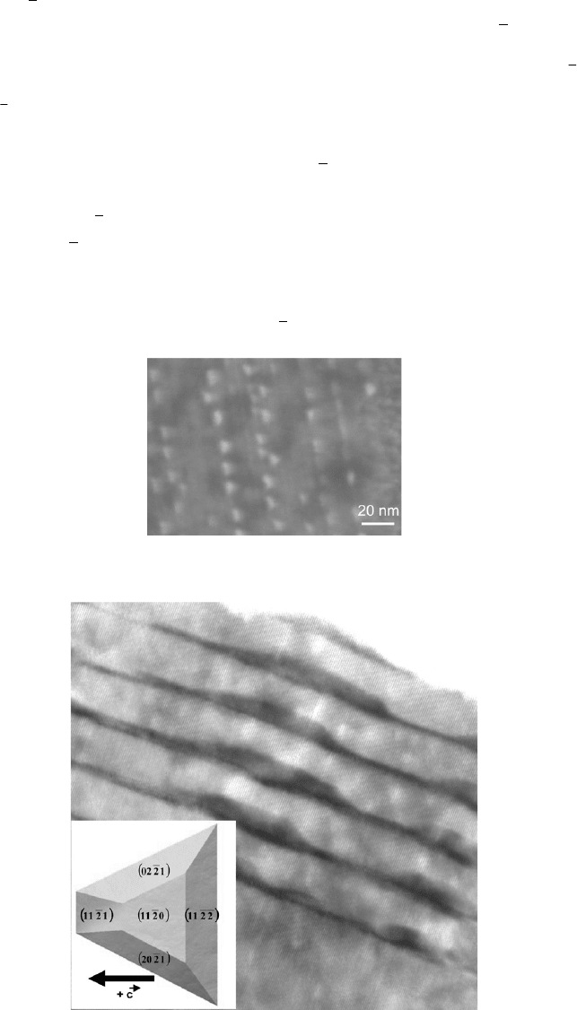
0] GaN QDs is more complex: scanning electron microscopy images shown
in Fig. 6.10 illustrate an asymmetry of dots along the [0001] polar direction. As a whole, various
shapes of dots have been identifi ed, from triangular to trapezoidal. Combined with HRTEM exper-
iments shown in Fig. 6.11 and analysis of the facets shown in RHEED pattern, the shape shown
as an inset in Fig. 6.11 has been proposed for [11
2
0] GaN dots.
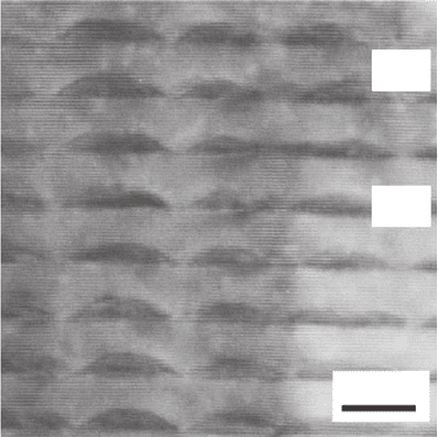
Figure 6.10 Scanning electron microscopy image of [11 2
–
0] GaN QDs. Note the coexistence of several shapes
(after [25] ).
Figure 6.11 HRTEM images of [112
–
0] GaN QDs viewed along the [11
–
00] zone axis. An asymmetry of the dots
is shown, i.e. two types of facets are seen along [0001] inclined by about 16° and 32° with respect to the basal plane
(after [25] ).
CH006-I046325.indd 209CH006-I046325.indd 209 6/27/2008 4:22:17 PM6/27/2008 4:22:17 PM
210 Handbook of Self Assembled Semiconductor Nanostructures for Novel Devices in Photonics and Electronics
The asymmetry of dots could be related to the direction of the [0001] polar axis by performing
convergent electron beam diffraction (CBED) experiments. As illustrated in the inset in Fig. 6.11,
it was demonstrated that triangularly shaped [11
2
0] GaN QDs point towards the c direction.
The dot asymmetry in the [0001] direction has been tentatively assigned to a faster growth rate
along c than along – c (see [25] ).
6.3 Structural properties of GaN QDs
The structural properties of QDs are delicate to carry out: either dots are let uncapped on the sub-
strate but may be modifi ed by oxidation or they are capped and the process of capping itself may
modify their chemical composition. It has been shown in section 6.2.2.2 that GaN QDs can be con-
sidered as a model system as no interdiffusion between dots and barrier has been seen to date. This
makes GaN QDs particularly suitable for study by HRTEM, medium energy ion scattering, X-ray dif-
fraction and Raman spectroscopy, which are the techniques usually used for obtaining insight into
dot structural properties and their variation as a function of capping and/or stacking. Note that
Raman spectroscopy is extensively presented in Chapter 7 and will not be considered further here.
6.3.1 [0001] GaN QDs
Among the techniques allowing one to characterize the structural properties of QDs, namely
their strain state with respect to the surrounding barrier, medium energy ion scattering (MEIS)
is a relatively new technique and has been used in a few cases to determine the strain profi le of
nanostructures at the monolayer scale [38, 39] . The principle of the technique is shown sche-
matically in Fig. 6.12 . It consists of measuring the angular and energetic distribution of medium
energy protons (typically 100 keV) backscattered from a target. As shown in Fig. 6.12 , the angu-
lar distribution exhibits dips aligned with crystallographic directions, which result from the
occurrence of a shadow cone for backscattered ions, due to the presence of atomic columns. The
angular position of this dip depends on the strain and may be easily related to the c/a ratio, c and
a being the out-of plane and in-plane lattice parameters, respectively. Due to the strong energy
loss of 100 keV protons, the depth resolution is as good as the monolayer, allowing one to extract
the strain profi le of buried/unburied QDs as a function of their height.
Ga
N
[0001]
100 keV incident H
beam
Angular distribution of
backscattered H
ions
Figure 6.12 S chematics of an MEIS experiment.
The case of GaN QDs covered by 20 ML of AlN, suffi cient to smooth AlN surfaces and consist-
ent with section 6.2.2.2, is shown in Fig. 6.13 and compared to theoretical calculations [40] .
CH006-I046325.indd 210CH006-I046325.indd 210 6/27/2008 4:22:18 PM6/27/2008 4:22:18 PM
Growth and Characterization of Structural and Optical Properties 211
Although the agreement is satisfactory, it has to be noted that the upper part of QDs is experi-
mentally found to be more relaxed than theoretically predicted, indicating that the effective QD
strain state likely depends partially on extrinsic parameters such as the presence of threading
edge dislocations in their close vicinity.
Alternatively, quantitative information on QD strain state may be obtained by performing
quantitative analysis of HRTEM images using the geometrical phase analysis technique [41, 42] .
The result for [0001] GaN QDs is displayed in Fig. 6.14 which shows maps of the local c and a lat-
tice parameters, respectively. From these images, it is inferred that compressed GaN QDs induce
strain in the surrounding AlN matrix. In particular, it is found that AlN above the dots exhib-
its an expanded a lattice parameter, i.e. AlN is in tension and constitutes a privileged nucleation
centre for the upper GaN dots, which leads to the build-up of vertical correlation of GaN QDs
discussed in section 6.4.
Combining the results in Fig. 6.14 , it is possible to extract a map of the c/a ratio value which
is also shown. An average value of 1.64 is found in the GaN QDs, allowing one to conclude that
GaN QDs are relaxed to a large extent, as c/a would be 1.69 in the hypothesis of a biaxial strain
and equal to 1.625 in a bulk GaN crystal.
If we now compare these HRTEM results with MEIS experiments previously discussed, a rather
good agreement is found. However, it should be noted that the sample preparation requested for
HRTEM experiments may lead to additional strain relaxation assigned to a thin foil effect.
6.3.2 [11
2
0] GaN QDs
It has been shown in section 6.2.2.3 that nucleation of [11
2
0] GaN QDs is highly anisotropic and
that dots are found to be aligned along the [1
1
00] direction. Their strain profi le was studied by
MEIS [43] . In that case, two perpendicular directions were used to measure the strain profi le in the
{ 0001 } and { 1
1
00 } planes, respectively (see Fig. 6.15 ).
The evolution of the
3
1120 1100
aa/
and
ac
1120
/
ratios as a function of depth is shown
in Fig. 6.16 . The data are compared to the case of a GaN layer completely strained in both in-
plane directions on a relaxed AlN [37] (labelled GaN/AlN in Fig. 6.16 ), and to the case of relaxed
GaN (corresponding to
31
1120 1100
aa/
in Fig. 6.16 a and
ac
1120
0 615/ .
in Fig. 6.16 b).
However, it is worth noting that the AN buffer layer which as been deposited on SiC prior to GaN
QD growth is probably far from being completely relaxed. In such a case, the strain state of GaN
should lie between that of GaN/relaxed AlN and that of GaN/SiC, in good agreement with experi-
mental results (see Fig. 6.16 ).
1.71
1.70
1.69
1.68
1.67
1.66
1.65
1.64
1.63
1.62
1.61
1.60
1.59
1.58
93.5 94.0 94.5 95.0 95.5 96.0 96.5 97.0
543210
(a)
QDs top
Relaxed c/a
Depth (nm)
Energy (keV)
Z (nm)
(b)
Relaxed c/a
c/a
c/a ratio
Biaxial c/a
10
1.58
1.60
1.62
1.64
1.66
1.68
1.70
123
Figure 6.13 (a) c/a profi le as a function of depth for GaN QDs covered by 20 MLs of AlN. (b) Theoretical
calculations (after [40] ).
CH006-I046325.indd 211CH006-I046325.indd 211 6/27/2008 4:22:18 PM6/27/2008 4:22:18 PM
212 Handbook of Self Assembled Semiconductor Nanostructures for Novel Devices in Photonics and Electronics
The evolution of the
3
1120 1100
aa/
ratio, corresponding to the strain profi le along [1
1
00]
( Fig. 6.16 a), puts in evidence a decrease of the strain from the GaN/AlN interface to the top of the
dots and wetting layer: while the initial value at the GaN/AlN interface is found to be larger than
the value of a completely strained GaN, the strain at the top of the dots is intermediate between the
completely strained and the relaxed values. We now turn to the evolution of the
ac
1120
/
ratio, cor-
responding to the strain profi le along [0001] ( Fig. 6.16 b). It appears that the initial strain value at
the GaN/AlN interface is lower than the corresponding initial value in the [11
2
0] direction.
As a whole, the strain profi les along the two non-equivalent [1
1
00] and [0001] directions are
remarkably different. The systematic enhanced strain relaxation at the base of the dots along
the [0001] direction has been interpreted as possibly due to a plastic process [43] . Indeed, in the
case of a GaN layer deposited on a relaxed AlN, the in-plane GaN strain at the GaN/AlN interface
amounts to 2.4% along [1
1
00] and 3.9% along [0001]. The greater in-plane strain along
0.47 0.49 0.5
c (nm) a (nm)
0.52 0.54 0.297 0.304 0.311 0.318 0.325
1.64071
1.59846
1.59714
1.65144
1.61347
1.5567
1.63224
1.55808
1.56815
1.61212
1.64319
1.5571
Figure 6.14 Maps of the whole 2 K 2 K CCD image shown in Fig. 6.12 . (a) Map of the c lattice parameter;
(b) map of the a lattice parameter; (c) c/a mapping extracted from results displayed in Fig. 6.13 a and b. Note that
the relaxed values of c and a are 0.5185 nm and 0.3189 nm, respectively, leading to a c/a ratio of 1.625.
CH006-I046325.indd 212CH006-I046325.indd 212 6/27/2008 4:22:19 PM6/27/2008 4:22:19 PM
Growth and Characterization of Structural and Optical Properties 213
[0001] could favour plastic strain relaxation through the formation of misfi t dislocations at the
GaN/AlN interface along the [0001] direction. These defects would partly account for the 3.9%
total strain, while additional elastic relaxation would accommodate part of the residual lattice
mismatch. The combination of these elastic and plastic relaxation mechanisms could account
for the smaller residual strain measured along [0001].
Interestingly, misfi t dislocations associated with this hypothetical plastic relaxation have been
observed by HRTEM, as evidence that misfi t dislocations are generated in order to accommodate the
stress in the [0001] direction. Very roughly, the lattice mismatch accommodated through the forma-
tion of these dislocations can be estimated at 1 to 2%. Note that this value is consistent with the neg-
ative offset of the strain profi le displayed in Fig. 6.16 b with respect to the one displayed in Fig. 6.16 a.
(a) (b)
[1100]
[0110]
[1121]
a
b
c
[0001]
a
1120
100 keV
incident H
a
1100
u
i
u
0110
u
1121
[1120]
Figure 6.15 Scheme of the scattering geometry in the [0001] (a) and [1 1
–
00] (b) planes for medium energy ion
scattering (after [43] ).
GaN/AIN
GaN/SiC
GaN/SiC
GaN/AlN
Depth (nm)
0
1
1.02
1.04
1.06
0.4 0.8 1.2 1.6 2 2.4 2.8
0.62
0.64
0.66
Relaxed GaN
(b)
Top of QDs
(a)
Top of QDs
Relaxed GaN
Figure 6.16 Depth profi le of the
3/ aa
1120 1100
(a) and a
112
–
0
/c (b) ratios for [112
–
0] GaN QDs. The GaN/
AlN label refers to a GaN layer completely strained in both in-plane directions on a relaxed AlN.
CH006-I046325.indd 213CH006-I046325.indd 213 6/27/2008 4:22:21 PM6/27/2008 4:22:21 PM
214 Handbook of Self Assembled Semiconductor Nanostructures for Novel Devices in Photonics and Electronics
6.4 Vertical correlation of stacked QDs
Vertical correlation of stacked QD planes is observed when the spacer between adjacent planes
is suffi ciently thin to ensure a modulation of the surface elastic potential induced by the pres-
ence of buried dots. As a consequence, nucleation of the upper QD plane preferentially occurs
in the regions of the spacer locally extended by the presence of dots below. This mechanism has
been described by Tersoff et al . [44] . It also works for GaN QDs and results in an homogeniza-
tion of their size distribution associated with an average size increase [45] . Figure 6.17 shows an
HRTEM image of vertically correlated GaN QDs planes embedded in AlN. The AlN spacer between
adjacent planes is about 6 nm.As discussed in section 6.3.1, such a spacer is thin enough to medi-
ate the deformation induced by the presence of the lower QD plane up to the surface. Moreover, it
has been consistently shown by Raman spectroscopy ( cf . Chapter 7) and by X-ray diffraction (see
section 6.5) that vertical correlation can be experimentally observed for an AlN spacer thinner
than about 8 nm.
AIN
GaN
8 nm
Figure 6.17 HRTEM image of a superlattice of vertically correlated GaN QD planes embedded in AlN.
It is worth noting that according to the model of Tersoff [44] , vertical correlation, far of
only consisiting of a vertical alignment of dots, implies an elastic interaction of the dot/barrier
system which eventually results in a size fi ltering of dots and an homogenization of their pop-
ulation. Such a behaviour is illustrated in Fig. 6.18 which displays photoluminescence (PL)
results of vertically correlated [0001] GaN dots as a function of the number of stacked planes. To
properly interpret the results in Fig. 6.18 , one must recall that optical properties of [0001]
GaN dots are dominated by the presence of an internal electric fi eld which results in a marked
red shift of PL energy (see Chapter 7). One consequence of the electric fi eld, which may be as
strong as 10 MV/cm, is to emphasize the dot size dispersion effect. This is seen in Fig. 6.18 where
the peak corresponding to three stacked planes of dots is as wide as 750 meV. For an increasing
number of planes, which are correlated to the build-up of vertical correlation, one observes both
(i) a drastic reduction in PL line width and (ii) an increased red shift whereas the left side of the
PL peak is almost unchanged. These variations are consistent with an increase in the average dot
size and an homogenization of dot population, as a signature of vertical correlation of succes-
sively stacked planes of dots. The driving force of the correlation has been identifi ed in Fig. 6.14 ,
i.e. the elastic deformation of the surrounding AlN barrier by GaN dots, acting as a nucleation
fi lter.
CH006-I046325.indd 214CH006-I046325.indd 214 6/27/2008 4:22:21 PM6/27/2008 4:22:21 PM
Growth and Characterization of Structural and Optical Properties 215
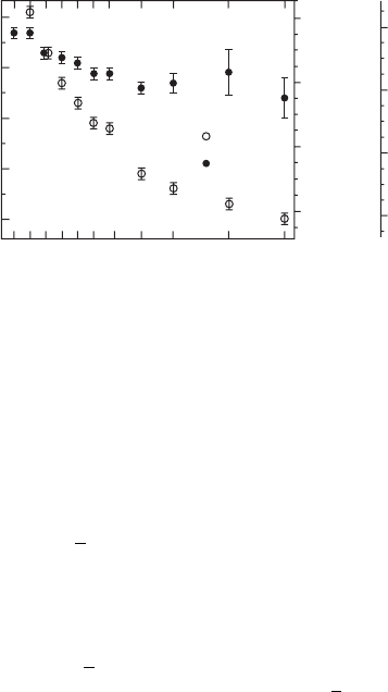
6.5 X-ray diffraction analysis of GaN QDs
Structural characterization of GaN QDs by X-ray diffraction deserves special attention for several
reasons. First of all, development of Synchrotron facilities has made feasible the characterization
of single QD planes, despite the small amount of material under consideration, typically a few
MLs. However, the epitaxial relationship between nanostructures and their substrate is a source
of additional diffi culties as both QDs and the substrate are diffracting in almost the same region
of reciprocal space, making diffi cult – if not impossible – the deconvolution of each contribution.
Furthermore, the situation is even more complicated due to the small size of QDs which leads to
a marked diffraction peak widening.
Most of these diffi culties can be overcome by the recent development of anomalous diffraction
techniques under grazing incidence. First of all, multiwavelength anomalous diffraction (MAD)
allows one to extract the structure factor of a specifi c element and, thus, the average strain,
composition, and size of the corresponding region [46] . Second, the fi ne structure oscillations
measured above the absorption edge in diffraction condition, known as extended diffraction
anomalous fi ne structure (EDAFS), provide the local environment of the absorbing atoms in the
diffraction-selected region [47] . Then, a proper combination of MAD and EDAFS makes possible
a comprehensive study of the strain state of nanostructures, allowing one to determine both in-
plane and out-of-plane strain.
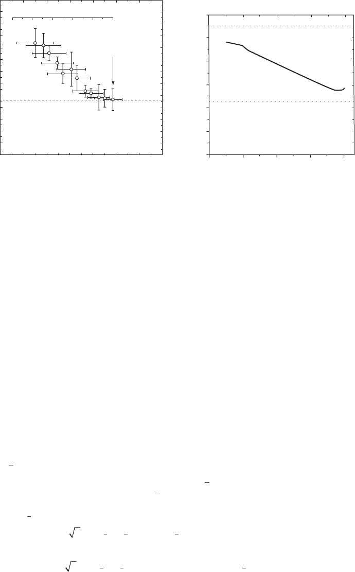
These techniques have been recently applied to the case of GaN QDs [48, 49] – Fig. 6.19 a
shows the diffracted intensity as a function of X-ray energy. In the case of uncapped GaN QDs
deposited on a thin AlN buffer on [0001] SiC, the Ga K edge is at 10.367 keV. Clearly, the inten-
sity of the shoulder on the edge of the peak at h 3 corresponding to SiC is strongly energy
dependent, as a chemical signature of the presence of Ga in diffracting material. Following an
extraction procedure described in [48] and [49] , the contribution of GaN is shown in Fig. 6.19 b.
The position of the Ga signal maximum along [10
1
0] is directly related to the average in-plane
strain state in the QDs.
By performing MAD experiments at the maximum of the Ga partial structure factor, as a func-
tion of the AlN deposit on top of the QD planes, it was possible to extract the x Al/Ga proportion
of the isostrain volume selected by diffraction [49] . The result is shown in Fig. 6.20 . Up to 4–5 ML,
the Al proportion, which is near to zero for free-standing QDs, increases linearly, and stabilizes
1
200
400
600
800
FWHM (meV)
GaN periods
1.5
0.0
0.2
0.4
0.6
0.8
1.0
3 periods
10 periods
50 periods
200 periods
Normalized PL
Energy (eV)
10 100
2.0 2.5 3.0 3.5 4.0 4.5 5.0
Figure 6.18 Photoluminescence of stacked GaN QDs planes as a function of the number of planes. Inset : Variation
of FWHM of photoluminescence peaks as a function of the number of stacked planes.
CH006-I046325.indd 215CH006-I046325.indd 215 6/27/2008 4:22:22 PM6/27/2008 4:22:22 PM
216 Handbook of Self Assembled Semiconductor Nanostructures for Novel Devices in Photonics and Electronics
above 4–5 ML, with a trend to saturate for further AlN coverages. Provided that AlN on top of the
QDs is pseudomorphic to GaN for low coverages [50] , and as no appreciable intermixing occurs
inside the GaN QDs [49, 33] , the variation of the Al proportion x in the isostrain region up to
4–5 ML indicates a uniform increase of the amount of AlN on top of the GaN QDs, followed by
a change in the AlN growth process, which leads to AlN with an in-plane strain state different
from that in the QDs. These results are consistent with the capping model described in section
6.2.2.2, as an illustration of the capabilities of anomalous diffraction techniques.
0
0.03
0.06
0.09
2.9
2.95
3
h (r.s.u.)
h (r.s.u.)
2.9 2.95 3
(a)
Scattered intensity (arb. units)
Bulk
GaN
Bulk
AIN
SiC
(b)
0
0.1
0.2
Scattered amplitude modulus
(arb. units)
Overall
Ga
10.467 keV
10.367 keV
10.357 keV
10.267 keV
Figure 6.19 ( a) Diffracted intensity measured at four energies across the Ga K edge at 10.367 keV, along the [101
–
0 ]
reciprocal space direction, labelled in reciprocal space units (r.s.u.) by h. h 3 is the position of the SiC substrate, used
as a scale reference. (b) Extracted modulus of the Ga region’s cattered amplitude, as deduced by MAD, compared to the
square root of the overall scattered intensity measured at 10.267 keV. Grazing incidence angle, α , 0.3° (after [49] ).
0 2 4 8 11 18
AlN deposit (ML)
x AI proportion (%)
20
15
10
5
0
Figure 6.20 Al proportion x of the isostrain region, as a function of the AlN deposit on top of the QD plane
(after [49] ).
Anomalous X-ray diffraction in grazing incidence has also been used in situ to determine the pro-
gressive strain changes in both GaN QDs and the AlN barrier as a function of AlN thickness [50] .
Results are shown in Fig. 6.21 . They illustrate the combined tension/compression in the interact-
ing AlN/GaN system. Interestingly, almost no strain variation is observed beyond an AlN thickness
of about 8 nm (1 ML is about 0.25 nm), as evidence that the “ memory ” of the subjacent GaN QD
plane is lost for thicker AlN layers. This result is consistent with the maximum AlN thickness which
was found to make possible vertical correlation of successive planes of dots (see section 6.4) and
also to Raman spectroscopy results leading to a similar conclusion (see Chapter 7).
CH006-I046325.indd 216CH006-I046325.indd 216 6/27/2008 4:22:23 PM6/27/2008 4:22:23 PM
Growth and Characterization of Structural and Optical Properties 217
6.6 Optical properties of single GaN QDs
After the physics of the growth and the study of the structural properties of GaN/AlN QDs, this
section discusses the optical properties of these heterostructures. The previous chapter described
in detail the optical properties of polar QDs. The following section focuses more particularly on the
optical properties of non-polar [11
2
0] QDs, with an emphasis on the photoluminescence experi-
ments on single quantum dots.
6.6.1 Photoluminescence of ensembles of non-polar GaN QDs
The overall optical properties of [11
2
0] quantum dots are not obvious to forecast. Indeed, in that
case, the polar axis ( c axis) is in the plane of the layers. For a [11
2
0] quantum well, the situation
is quite simple: the polar axis is parallel to the GaN/AlN interfaces. There is thus no discontinu-
ity of the polarization perpendicular to the interfaces so that there is no internal electric fi eld.
Despite the wurtzite cell, a non-polar quantum well thus behaves like a “ standard ” quantum well
for which only confi nement effects are present. This was confi rmed experimentally in several
publications [51, 52] .
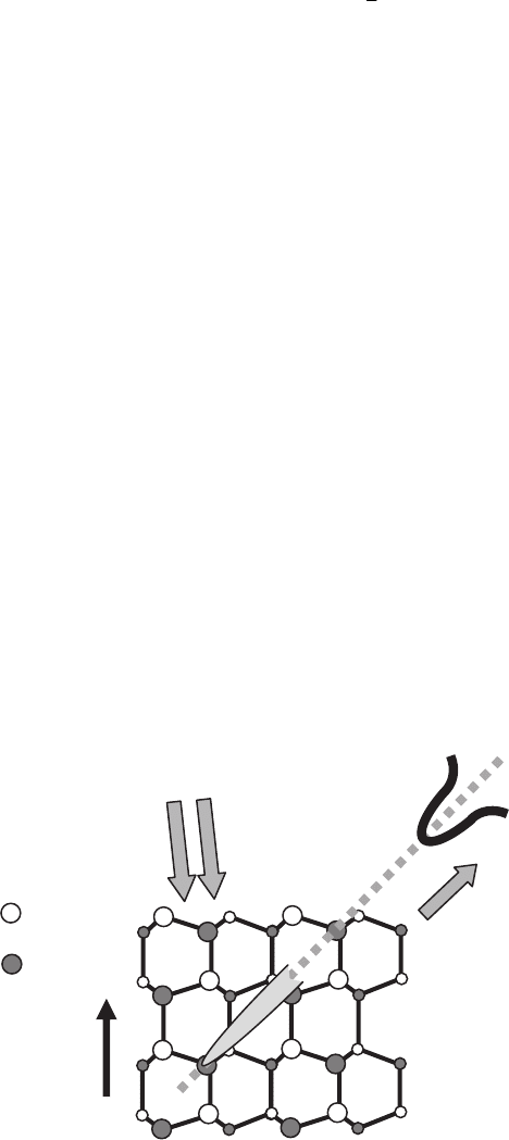
For quantum dots, the situation is more complicated. Indeed, the polarization vector does have
a component along the normal to the quantum dot lateral facets. Therefore, a sheet charge den-
sity due to this polarization discontinuity appears on the QDs lateral facets. This charge density
will thus generate an internal electric fi eld that is likely to induce a sizeable quantum confi ned
Stark effect. The geometry of the situation is, however, very different from the situation of polar
QDs and QWs.
For polar heterostructures, the sheet charge densities created by the polarization discontinui-
ties form a “ condensator-like ” structure in which two charged planes face each other giving rise
to a quasi-uniform electric fi eld inside the confi ned structure (even for quantum dots). For non-
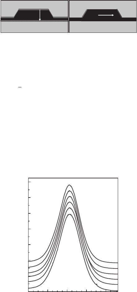
polar quantum dots, the geometry is quite different (see Fig. 6.22 ): only the two side facets of
the QDs that are crossed by the c -axis carry a charge. This is thus a three-dimensional electro-
static problem, and the precise determination of the internal electric fi eld requires the knowledge
of the dot geometry, the strain distribution and the residual doping of the samples. Preliminary
calculations by A. Cros and co-workers (see Chapter 7) have shown that the electric fi eld should
be much reduced (by at least one order of magnitude) compared to polar quantum dots [53] .
Let us note that the issue of the residual doping of the quantum dots (usually MBE-grown non-
intentionally doped III-N structures show a n-type character) is crucial here as it can be shown
that each lateral facet of a non-polar dot carries the equivalent of between one and two elemen-
tary charges, so that the presence of a few electrons in each dot can drastically screen the inter-
nal electric fi eld.
AlN coverage (MLs)
02468101216 20 27
0.6
1
1.4
1.8
0.6
1
1.4
1.8
34
3.13
3.14
3.15
3.16
3.17
a(Å)
AlN
GaN
f
GaN
(%)
f
Al N
(%)
Figure 6.21 In-plane lattice parameter and mismatches – relative to bulk AlN or GaN – for AlN and GaN deduced
from F
Al N
and F
Ga
extractions. The error bars in the last three points for GaN are large due to weak extracted F
Ga
(after [50] ).
CH006-I046325.indd 217CH006-I046325.indd 217 6/27/2008 4:22:23 PM6/27/2008 4:22:23 PM
218 Handbook of Self Assembled Semiconductor Nanostructures for Novel Devices in Photonics and Electronics
The a priori determination of the optical properties of these non-polar QDs being a complex
task requiring a precise knowledge of the structural and electronic properties of the grown struc-
tures, our approach was to probe experimentally the effect of the internal electric fi eld on the
optical properties of the [11
2
0] quantum dots.
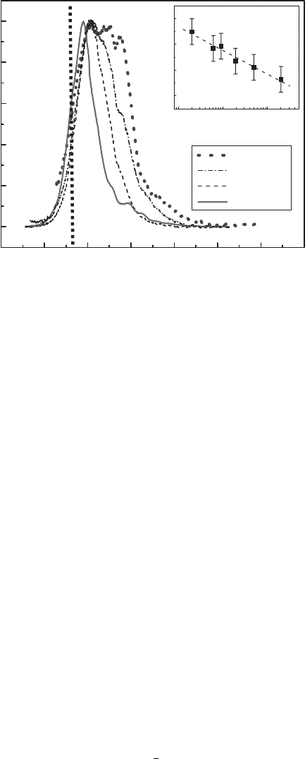
The fi rst experiment ( Fig. 6.23 ) was to perform a low-temperature (5 K) photoluminescence
experiment on an ensemble of QDs, as a function of excitation power density. The sample is
excited with a cw doubled argon laser, emitting at 244 nm (5.1 eV). The excitation power is var-
ied over more than fi ve orders of magnitude; the curves are vertically offset for clarity. The fi rst
observation is that the photoluminescence occurs above the GaN band gap, so that the confi ne-
ment effects dominate over the quantum confi ned Stark effect. This is quite unlike polar quan-
tum dots of similar sizes for which the quantum confi ned Stark effect leads to a spectacular red
shift of the luminescence of the QDs, which can be up to 500 meV below the GaN band gap [54,
27] . Moreover, there is no indication of screening over the range of excitation densities that was
probed. Again this is unlike polar GaN QDs for which the screening of the internal fi eld by the
photocreated carriers is observable over a wide excitation density range [55] .
GaN
AlN
AlN
+
++
+
+
+ +
+ + +
+
+ +
+
+ +
+
-
-
-
-
-
-
-
-
-
-
-
-
-
-
-
-
-
E
GaN
AlN
+
-
E ?
AlN
Figure 6.22 Geometry difference between a polar QD and a non-polar QD. On the left, a polar QD ( c -axis pointing
upwards), with planar capacitor-like geometry. On the right, a [112
–
0] QD ( c -axis in the plane of the page, pointing
leftward) with few charges deposited on two side facets. The typical QD size is 20 nm diameter and 2 nm height.
3.4
P ⴝ 3 mW/cm
2
P ⴝ 30 mW/cm
2
P ⴝ 300 mW/cm
2
P ⴝ 1 W/cm
2
P ⴝ 10 W/cm
2
Normalized intensity (a.u.)
Ener
g
y (eV)
T ⴝ 5 K
P ⴝ 100 W/cm
2
3.6 3.8 4.0 4.2
Figure 6.23 Photoluminescence spectrum at 5 K for various excitation power densities (at λ 244 nm). The
luminescence is above the GaN band gap, and no screening effect is observed in this excitation power range.
The most convincing experiment to probe the quantum confi ned Stark effect is to measure
the radiative lifetime of the confi ned excitons, which is very sensitive to the spatial separation
of electrons and holes. This is especially true for non-polar structures as the two charged planes
are spatially well separated (by one QD diameter): in that case even a small internal electric fi eld
will separate the electron and hole wavefunctions and thus reduce drastically the transition
oscillator strength, while the energy of the transition would be little affected. The time-resolved
CH006-I046325.indd 218CH006-I046325.indd 218 6/27/2008 4:22:23 PM6/27/2008 4:22:23 PM