Gross R., Sidorenko A., Tagirov L. Nanoscale Devices - Fundamentals and Applications
Подождите немного. Документ загружается.


Quasioptical Terahertz Spectrometer Based on a Josephson Oscillator 327
heating with unavoidable degradation of the sensitivity. Practical TES
sensors sacrifice sensitivity to avoid saturation.
Superconducting Tunnel Junctions (STJ) of the Superconductor-
Insulator-Superconductor (SIS) type, as well as Superconductor-Insulator-
Normal metal (SIN) type can be used from microwave to X-ray wavebands.
They are currently being developed as photon counting detectors. STJ
convert the incident radiation energy into a population of excited charges
whose number is proportional to the deposited energy and to the inverse of
the superconducting gap. The superconducting electrode in which this
conversion takes place serves as absorber. By measuring the tunnel current
it is possible to estimate the incoming energy and frequency [4]. Due to the
finite leakage current and quantum efficiency about unity, the best NEP is
about 10
-16
W/Hz
1/2
.
The Superconducting Hot Electron Bolometer (SHEB) is mainly used in
HEB mixers as a relatively fast (up to 10 GHz) power meter of interfered
signal and LO waves, and in general it is the same type of power detector,
because at signal and LO frequencies it is too slow and can’t multiply these
components. It has a very low thermal capacitance and a large thermal
conductance, and in this way it is optimized for speed, but not for
sensitivity. This type of sensor can be optimized for direct detection, a so-
called Hot Electron Direct Detector (HEDD). The theoretical estimations of
NEP below 10
-20
W/Hz
1/2
[5] seems to be very optimistic. Taking into
account the background power load, HEDD NEP should be limited at the
same thermodynamic level of above 10
-18
W/Hz
1/2
.
The Normal metal Hot Electron Bolometer with Andreev mirrors
(ANHEB) was proposed by M. Nahum and P.L. Richards [6] and consists
of a thin normal-metal strip between superconducting electrodes. Low
electron-phonon interaction at low temperatures together with Andreev
reflection at the boundary of a normal metal and a superconductor prevent
heat leakage from hot electrons to phonons and to the electrodes. A
superconductor-insulator-normal metal (SIN) junction attached to the
normal metal strip is used for temperature sensing. The best NEP=5
.
10
-18
W/Hz
1/2
was achieved at 100 mK [7].
The SINIS normal metal cold electron bolometer (CCNHEB or CEB)
was proposed in [8] and experimentally demonstrated in [9]. As in all
previous cases, the responsivity and noise equivalent power (NEP) of the
bolometer are mainly determined by its electron temperature. To improve
CCNHEB
performance it was suggested using direct electron cooling of
the
absorber by a superconductor-insulator-normal metal (SIN) tunnel

328 M. Tarasov, L. Kuzmin, E. Stepantsov, A. Kidiyarova-Shevchenko
junction [10]. The effect of electron cooling was demonstrated in [11]. The
CEB is essentially a nanorefrigerator that cools the electrons within a thin
metal film by extracting the hottest electrons through SIN junctions. This
effect is similar to that used in a thermoelectric cooler (Peltier effect). In
contrast to TES, an unavoidable dc heating for electrothermal feedback is
replaced by a deep electron cooling, removing all incoming power from the
absorber to the next stage. Thereby the electron temperature is maintained
at the minimum level below the phonon temperature independently on the
relatively high power load. The refrigeration effect allows this detector to
operate with high sensitivity under high power load. The response time is
determined by the tunneling time of electrons which can be very fast
(∼10ns).
The NISIN hot electron bolometer [12] is completely complementary to
the SINIS bolometer and clarifies the difference between hot electron and
cold electron bolometers. In the NISIN case a photon assisted tunneling
through the barrier heats the middle S electrode. Hot electrons are injected
into a superconductor; they reduce the energy gap, which in turn increases
the current through the junction.
The Kinetic Inductance Bolometer (KID) is based on the fast change of
the kinetic inductance in a superconducting strip when a pair breaking
process reduces the superfluid density [13]. The basic principle of operation
of the KID is to measure the resonant frequency of a thin-film
superconducting resonator, operating at about 5 GHz. The frequency shift is
detected by monitoring the transmission or reflection phase, and this shift is
proportional to the energy of the absorbed photon. According to [14] the
NEP is determined by the quasiparticle generation-recombination noise and
at T~1K it can be as small as 10
-19
W/Hz
1/2
, again without accounting for
the background power load.
Among these six generic superconducting bolometers the majority is
operated at an electron temperature that is equal or above the bath or
phonon temperature. Only the CEB works at a reduced electron
temperature. Moreover, the electron cooling allows extracting the heating
power, which leads to an increase of the saturation level. As a result the
effect of the background power load is not as severe as for the rest of
bolometer types.

Quasioptical Terahertz Spectrometer Based on a Josephson Oscillator 329
Samples Layout and Fabrication
A general view on the cold electron bolometer with capacitive coupling
(CCNHEB) chip is presented in Fig. 1. One can see in the center a
broadband log-periodic antenna for
the frequency range 0.1-2 THz, and
double-dipole antennas for 300 and 600 GHz to the left and to the right
from the center. Besides above and below the central antenna there are two
structures with additional SIN junctions for studies of electron cooling in
SINIS structures. The first step of sample fabrication was thermal
evaporation of 60 nm Au for fabrication of the normal metal traps and
contact pads. The pattern for the traps and the pads were formed using
photolithography. The next step was the fabrication of the tunnel junctions
and the absorber. The structures were patterned by e-beam lithography and
the metals were thermally evaporated using the shadow evaporation
technique. The Al (superconductor) was evaporated at an angle of about
60° up to a thickness of 65 nm and oxidized at a pressure of 10
-1
mbar for 2
minutes. A Cr/Cu (1:1) absorber of a total thickness of 75 nm was then
evaporated directly perpendicular to the substrate. The cooling junctions
have a normal state resistance R
N
equal to 0.86 kΩ, while the two inner
junctions have R
N
equal to 5.3 kΩ. The inner junctions have a simple cross-
type geometry, where a section of the normal metal absorber overlaps the
thin Al electrodes. The area of overlap, which determines to the area of
each of the tunnel junction, is equal to 0.2 x 0.3 µm
2
. The structure of the
outer junctions is such that the ends of the normal metal absorber overlap
with a corner of each of the Al electrodes, which have a much larger area
compared to the middle Al electrode. The area of each of these junctions is
0.55 x 0.82 µm
2
. The purpose of the larger area Al electrode is to provide
more space for quasiparticle diffusion compared to the middle Al electrode
with simple cross-type geometry. In the described structure, the two outer
and inner junctions have the R
N
equal to 0.85 kΩ and 5.4 kΩ, respectively.
The volume of the absorber was 0.18 µm
3
.
A bias cooling current is applied through the outer junctions and the
absorber. These tunnel junctions act as the cooling junctions, and therefore
serve to decrease the electron temperature of the absorber. To determine the
electron temperature, the voltage across the inner junctions is measured. A
small current bias is applied to these junctions. The bias has to be optimal
to obtain the maximum linear voltage response on temperature, and yet not
too large so as to disturb the cooling process in the absorber.

330 M. Tarasov, L. Kuzmin, E. Stepantsov, A. Kidiyarova-Shevchenko
High critical temperature Josephson junctions on tilted bicrystal sapphire
substrates were fabricated in YBaCuO epitaxial films with the c-axis
inclined in <100> direction by angle 14
o
+14
o
. Films 250 nm thick were
deposited by pulsed laser ablation on tilted sapphire bicrystal substrates
covered by a CeO
2
buffer layer. The critical temperature of the film was
T
c
=89 K and ∆T
c
=1.5 K. Bicrystal Josephson junctions with a width
ranging from 1.5 to 6 µm demonstrated a characteristic voltage I
c
R
n
of over
4 mV at a temperature of 4.2 K. This makes them promising candidates as
oscillators for Terahertz frequency band applications.
Fig. 1. Optical micrograph of the central part of the CEB chip.
Power and Temperature Responses of the Bolometer
We measured the temperature response of the bolometers at temperature
down to 260 mK. The dc response was measured at upper and lower
structures with four SIN junctions. Two external junctions were used as
thermometers and two internal as heaters. The highest measured value of
the voltage response to temperature variations is over 1.6 mV/K and the
largest current response about 37 nA/K for a 10 kΩ junction and 55 nA/K
for a 6 kΩ junction.
It was possible to apply a dc power to the central pair of junctions and
measure the response of the outer pair of SIN junctions for these samples
with four SIN junctions. We observed the largest voltage response of

Quasioptical Terahertz Spectrometer Based on a Josephson Oscillator 331
400 V/µW for a 70 kΩ junction and 550 A/W for a 10 kΩ junction. The
obtained values of current and voltage responses can be converted to the
natural figure of merit for the sensitivity of the bolometer, namely the Noise
Equivalent Power (NEP):
NEP=I
n
/S
i
or NEP=V
n
/S
v .
11
V
/
0.8 10 /
/
PVT
GWK
TVP
−
∂∂∂
== =⋅
∂∂∂
Now we can calculate the thermodynamic NEP arising from the electron-
phonon interaction NEP
ep
2
=4kT
2
G in which the thermal conductivity
G=5Σ
ν
T
4
=10
-11
W/K,
ν
is the absorber volume. This results in a
thermodynamical noise equivalent power NEP
TD
=1.4
.
10
-18
W/Hz
1/2
and, if
we compare with the thermal conductivity in the voltage bias mode, it
corresponds to a NEP
V
=1.3
.
10
-18
W/Hz
1/2
.
Irradiation of Bolometer by a Josephson Junction
To increase the output microwave power from the Josephson junction and
increase the oscillation frequency it is necessary to increase the critical
current of the Josephson junction. Placing the Josephson junction on the
He4 stage prevents the sample from overheating by the relatively high
power absorbed by the Josephson junction. For example, if we take a
junction with 10 kΩ normal resistance and an oscillation frequency of
300 GHz, this results in an absorbed power over 0.2 µW. At 1 THz it is
already 2.5 µW.
Here, I
n
is the current noise, V
n
is the voltage noise, S
i
=dI/dP is the current
response, S
v
=dV/dP is the voltage response of the bolometer. Taking the
voltage noise of a room-temperature preamplifier of about 3 nV/Hz
1/2
one
can obtain the technical TNEP value to TNEP=1.25
.
10
-17
W/Hz
1/2
Using measured values of the temperature response and the power
response one can also obtain the thermal conductivity of the bolometer.
332 M. Tarasov, L. Kuzmin, E. Stepantsov, A. Kidiyarova-Shevchenko
0.00.20.40.60.81.01.21.41.6
0
2
4
6
8
Response,
µ
V
Frequency, THz
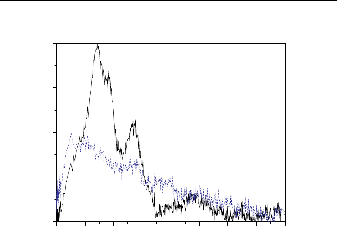
Fig. 2. Response measured by double-dipole and log-periodic antennas for the
same radiation source.
The layout of the Josephson sample was with similar log-periodic
antennas, and the critical current was over 500 µA at 2 K. As a result the
I
c
R
n
product exceeds 5 mV for non-hysteretic junctions and such oscillators
can in principle operate at frequencies above 2.5 THz. The experimental
curves shown in Fig. 2 have been measured by bolometers integrated with
double-dipole and log-periodic antennas. They reveal that there is a clear
maximum at the design frequency of 300 GHz for DDA and a smooth
spectrum for LPA. The response at higher bias voltages for the Josephson
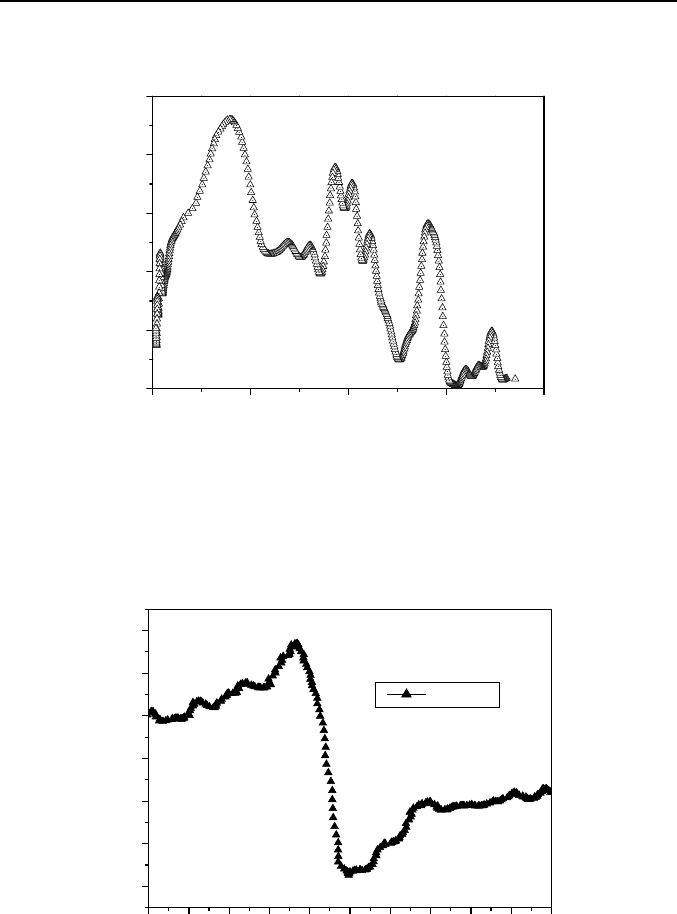
oscillator is presented in Fig. 3. The highest maximum corresponds to an
oscillation frequency of 1.75 THz.
For measurements at frequencies below 600 GHz we use also a low Tc
Josephson oscillator with resistively shunted Nb SIS tunnel junction. It is
integrated with the log-periodic antenna designed for 0.2-2 THz. Samples
were fabricated by HYPRES 3 µm Nb process (for details see
www.hypres.com). The linewidth of Josephson oscillations was measured
by irradiating such junction by a backward wave oscillator and monitoring
the detector response by a lock-in amplifier. The selective detector response
in Fig. 4 shows the voltage distance between bipolar maxima below 1 µV
that corresponds to the Josephson oscillations linewidth below 0.5 GHz.
Quasioptical Terahertz Spectrometer Based on a Josephson Oscillator 333
0.0 0.5 1.0 1.5 2.0
0.2
0.4
0.6
0.8
1.0
1.2
Response,
µ
V
Frequency, THz
Fig. 3. Response measured for high bias voltages of the Josephson junction. Last
maximum corresponds to an oscillation frequency of 1.75 THz.
425 426 427 428 429 430 431 432 433 434 435
-300
-200
-100
0
100
200
300
HYPRES A21 J2
measured 30.08.2004
T=1.8 K
BWO
∆V=1µV
Response, nV
Voltage, µV
RESP89
Fig. 4. Selective detector response of a Nb shunted tunnel junction at 215 GHz
with voltage distance between the maxima of about 1 µV corresponding to the
linewidth of 0.5 GHz.
334 M. Tarasov, L. Kuzmin, E. Stepantsov, A. Kidiyarova-Shevchenko
Conclusion
We demonstrated the first experimental response of a normal metal cold
electron bolometer at frequencies up to 1.7 THz. The noise equivalent
power of the bolometer is 1.3
.
10
-17
W/Hz
1/2
. We use an electrically tunable
high critical temperature Josephson quasi-optical oscillator as a source of
radiation in the range 0.2-2 THz and a shunted Nb SIS Josephson junction
for frequencies below 600 GHz. The combination of a Terahertz-band
Josephson junction and a high-sensitive hot electron bolometer opens the
possibility to develop a quasioptical cryogenic transmission spectrometer
with a resolution below 1 GHz. Such cryogenic spectrometer can be used
for low-temperature spectral evaluation of biological and chemical samples.
Cold electron bolometers can be used for remote atmosphere monitoring for
pollution detection, etc.
Acknowledgments
This work has been supported by Swedish agencies VR, STINT, and by
INTAS-01-686.
References
1. Richards PL (1994). J Appl Phys 76:1
2. Kuzmin L (2004). Proc. 15th Int Symp on Space Terahertz Technology,
Northampton, April 27-29
3. Irwin KD, Hilton GC, Wollman DA, Martinis J (1996). Appl Phys Lett
69:1945
4. Peacock A, Verhoeve P, Rando N, et al (1997). J Appl Phys 81:7641
5. Gershenson ME, Gong D, Sato T, Karasik BS, Sergeev AV (2001). Appl Phys
Lett 79:2049
6. Nahum M, Richards PL, Mears CA (1993). IEEE Trans Appl Supercond
3 :2124
7. Chouvaev D, Kuzmin L (2001). Physica C 352 :128
8. Kuzmin L (2000). Physica B 284-288 :2129
9. Tarasov M, Fominsky M, Kalabukhov A, Kuzmin L (2002). JETP Lett 76 :507
10. Kuzmin L, Devyatov I, Golubev D (1998). Proc. SPIE 3465:193
11. Nahum M, Eiles TM, Martinis JM (1994) Appl Phys Lett 65 :3123

Quasioptical Terahertz Spectrometer Based on a Josephson Oscillator 335
12. Barends R, Gao JR, Klapwijk TM (2004) 6-th Eur. Workshop on Low Temp
Electronics (WOLTE-6). 23-25 June, ESTEC, Noordwijk, The Netherlands, pp
25-31
13. Grossman E, McDonald D, Sauvageau J (1991). IEEE Trans Magn 27 :2677
14. Sergeev AV, Mitin VV, Karasik BS (2002). Appl Phys Lett 80 :817
NOVEL MATERIALS FOR ELECTRONICS