Gross R., Sidorenko A., Tagirov L. Nanoscale Devices - Fundamentals and Applications
Подождите немного. Документ загружается.

Superconducting/Ferromagnetic Nanostructures 229
thickness are measured with a quartz deposition controller with an accuracy
of 1 Å. The normal metal is either Ag, Pt, Pd or Pd
1-x
Ni
x
.
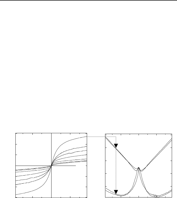
Pd is a highly paramagnetic metal and only few percents of Ni impurities
are necessary to drive it into the ferromagnetic state. We probe the onset of
ferromagnetism by Anomalous Hall Effect (AHE) on Pd
1-x
Ni
x
thin films
deposited on a bare substrate. The Hall resistance (i.e. V
Hall
/I) is reported in
Fig. 1a for diffrent Ni concentration ranging from 2.4 to 10%, an
anomalous component proportional to the magnetization appears for a Ni
concentration higher than 2.4%, as observed in bulk Pd
1-x
Ni
x
, while a
hysteresis in the Hall resistance appears for 7% (not shown). The Ni
concentration is determined by Rutherford Back Scattering spectrometry. In
Fig. 1b the magnetoresistance for the highest Ni concetration of Fig. 1a is
also reported. The magnetic field is oriented either in the film plane but
perpendicular to the current or perpendicular to the film plane. A strong
anisotrpy is observed, this anisotropy appears at concetration higher than
2.4% Ni together with the AHE. The hysteresis on the magnetoresistance is
not of magnetic origin, it results from fluctuations of the bath temperature.
Fig. 1. a) Hall resistance for different Ni concentrations. An anomalous Hall
component (AHE) appears at 2.5 % Ni. b) The anisotropy of magnetoresistance.
The paramagnetic regime
Figure 2 shows the tunnel conductance of CE/I/N/S junctions with pure Ag,
Pt, Pd and Pd
0.988
Ni
0
.
012
as a normal metal. The main feature of the
conductance is a minigap, E
g
. Note that the minigap decreases when the
susceptibility of the metal increases as expected by faster dephasing. In
Fig. 2 are also shown the fits (blue lines) of the conductance by the DOS
-0.3
-0.2
-0.1
0.0
0.1
0.2
0.3
R
xy
(ž)
-0.4
0.0
0.4
H
(
T
)
T=1.3K
2.4 %
9.8 %
-0.4
-0.2
0.0
0.2
0.4
∆
R
-0.4
0.0
0.4
H
(
T
)
Field ⊥
Field //
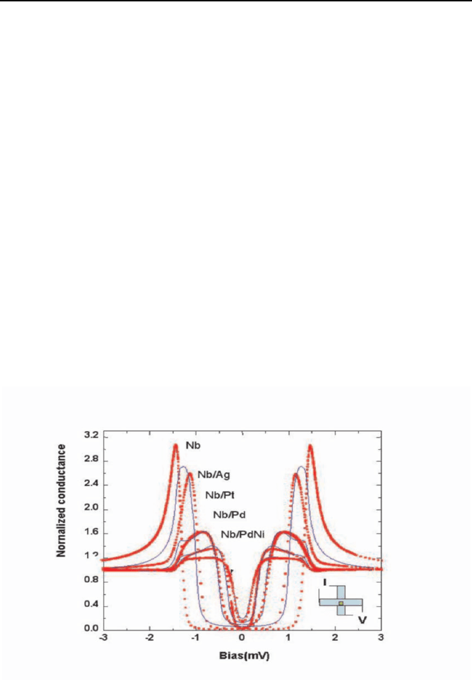
230 M. Aprili, M. L. Della Rocca, T. Kontos
found solving the Usadel equations. We used a self consistent code to solve
equation (1) together with the usual boundary conditions [9]. It turns out
that a finite
N
∆ is unnecessary to account for the data and that an upper
bound for the coupling constant
N
λ
is -0.1.
A finite interface resistance of about 5.10
-4
µ
Ω
cm
2
was used to account
for both the shape and the value of the energy gap for pure Pd. This value is
consistent with the one measured in Nb/Pd/Nb Josephson jutions [10]. This
finite resistance is supposed not varying when changing material and
remains also constant when adding Ni impurities in Pd. From the fits we
obtained
sf
λ
= 0.05, 2.05, 4.15, 5.3 for Ag, Pt, Pd and Pd
0.988
Ni
0.012
,
respectively. The electron-spin fluctuation coupling constant increases
between Ag and Pt and between Pt and Pd. It increases further when
increasing the Ni concentration as expected since the magnetic
susceptibility increases below the paramagnetic-ferromagnetic transition
consistently with specific heat data. Even though the precise relationship
between
sf
λ
and the Stoner enhancement is model dependent, a rough
estimate of it is given by
sf
λ
~2 (1-1/S)\lnS, where S is the Stoner factor.
This yields a Stoner factor of 10 for Pd, 3.3 for Pt and 1 for Ag, in
surprisingly good agreement with the known values for these metals.
Fig. 2. The superconducting density of states induced in a normal metal by the
proximity effect (red dots). The density of states of pure Nb is also shown. The fits
(blue lines) are obtained by solving the Usadel equations self consistently as
indicated in the text. In the inset the four probes cross geometry of the tunnel
junction is presented.
Superconducting/Ferromagnetic Nanostructures 231
The ferromagnetic regime
For Ni concentrations higher than 5.5%, the tunnel conductance displays
only one characteristic energy,
∆
, of about 1.35 meV, while the shape of
the spectra remains roughly the same. This is shown in Fig. 3, where all the
spectra have been scaled to the DOS corresponding to 5.5% of Ni. As finite
size effects vanished altogether, the proximity bilayer becomes similar to
that of a semi-infinite mesoscopic system
FF
d
ξ
> . The overall amplitude is
smaller than 5% of the background conductance and therefore it is possible
to find an analytical expression for the DOS and extract directly the value
of the exchange field in the Pd
1-x
Ni
x
layer. Linearizing eq. (2) we find the
following DOS:
[]
0
( ) 1 ( ) 1 exp( 2 / )cos(2 / )
ex th ex th
NE NE EE EE=+ − − ,
(3)
where N
o
(E) is the DOS at the Nb/Pd
1-x
Ni
x
boundary. We found
ex
E = 0.1,
0.5, 2.8, 3.3, 3.9 for 5.5%, 6%, 7%, 9.8%, 11.5% Ni, respectively.
Fig. 3. The proximity effect tunneling spectroscopy in a weak ferromagnet (PdNi)
is presented. The spectra are normalized by the PdNi exchange energy. The red line
is the best fit using the analytical expression.

232 M. Aprili, M. L. Della Rocca, T. Kontos
Therefore superconductivity is a very sensitive probe of
ex
E provided that
the size of the magnetic domains is larger than the superproduction
coherence length. On other words, the spatial resolution of a «Cooper pair
ex
E sensor» is given by
0
ξ
.
Spontaneous Vortices in Ferromagnetic Josephson
Junctions
In the ferromagnetic regime for a Ni concentration of about 10% the
superconducting wave function oscillates in F on a length scale given by
F
ξ
≈20 Å. A negative critical current occurs when the ferromagnetic thin
layer is coupled with a second superconductor and the superconducting
wave function is negative, originating
π
-coupling [11]. By shorting a
ferromagnetic
π
-junction with a 0-junction, a spontaneous supercurrent
sustaining half a quantum vortex occurs. We have detected such a current
by measuring the related phase gradient. The ground state of the 0-
π
junction is doubly degenerate, so that either half a quantum vortex or half
a quantum antivortex appears. As no coupling is observed at low
temperature between the two levels, the junction can be seen as the classical
limit of a two level system. It behaves macroscopically as a magnetic
nanoparticle of quantized flux, the magnetic anisotropy axis being defined
by the junction plane.
Device Design
The
π
-junction in a superconducting loop behaves as a phase bias
generator producing a spontaneous current and hence a magnetic flux. In
the limit 2
π
LI
c
<
0
Φ , the system gains energy by minimizing its magnetic
energy against the junction energy. The system maintains a constant phase
everywhere and a shift of
0
Φ
/2 in the current-phase relationship of the
junction is expected. On the other hand, when 2
π
LI
c
>>
0
Φ
the system's
minimum energy corresponds to that of the junction while maximizing its
magnetic energy. A phase gradient is maintained by generating a
spontaneous superconducting current, which sustains exactly half a
quantum flux. The ground state is degenerate as, the spontaneous
supercurrent
can circulate clockwise and counterclockwise with exactly
the same probability. Applying a small magnetic field can lift the
degeneracy and define an easy magnetization direction. The existence of a
Superconducting/Ferromagnetic Nanostructures 233
spontaneous supercurrent sustaining half a quantum flux in
π
-rings has
been recently shown in Nb loops interrupted by a ferromagnetic (PdNi)
π
-
junction [12]. Analogously, in a highly damped single Josephson junction
fabricated with a 0 and a
π
-region in parallel, a spontaneous half quantum
vortex is expected at the 0-
π
boundary.
The way we detect such a spontaneous supercurrent is by measuring the
phase gradient by a phase sensitive device, a second Josephson junction.
The ferromagnetic 0-
π
junction (source) and the detection junction
(detector) are coupled, as schematized in Fig. 4a, by sharing an electrode.
I.e., the top electrode of the detector Josephson junction is simultaneously
the bottom electrode of the ferromagnetic one. If half a quantum vortex is
spontaneously generated in the ferromagnetic junction, the spontaneous
supercurrent sustaining it circulates in the common electrode [Nb2, Fig. 4a]
producing a phase variation equal to
π
/2. A
π
/4-shift of the detection
junction's magnetic diffraction pattern is thus produced.
Fig. 4. a) Device geometry b) I-V characteristic of the detector junction.
When an external magnetic field is applied, in the hypothesis that the
thickness of the common electrode, Nb2, is comparable to the penetration
depth, the diffraction pattern of the detection junction is given by:
I(B)
=
I(0)
sin((
π
/
0
Φ
)(
sk
+
'
k
'
Φ
+
Φ
))
(
π
/
0
Φ
)(
s
k
+
'
k
'
Φ
+Φ
)
,
(4)
where
''
B
DtΦ= and
B
DtΦ= are the magnetic fluxes through the
ferromagnetic and detection junction respectively, with D the junction
width, t and t' the effective barrier thickness. J
s
is the spontaneous
supercurrent density, k
s
=0.5(
2
0
µ
λ
)D and k’=(
2
0
l
µ
)/L(D/wd
Nb2
) with
0
µ
the vacuum permittivity,
λ
the penetration depth, L the ferromagnetic
junction inductance, w the junction length and d
Nb2
the thickness of the
common electrode. The term k
s
J
s
generates the shift due to the spontaneous
supercurrent contribution, while the term k’
'
Φ
reduces the diffraction
-5
0
5
I (mA)
-4 -2 0 2 4
V (mV)
T = 1.5K
B = 0
Detector
A
l
SiO
SiO
I+
I-
V-
V+
Nb2
Nb1

234 M. Aprili, M. L. Della Rocca, T. Kontos
pattern period as a result of the contribution due to the screening current in
the ferromagnetic junction.
Device Fabrication
Samples are fabricated as described above for the single tunnel junctions.
First the bottom planar Nb/Al/Al
2
O
3
/Nb detection junction is made. A
1000 Å thick Nb [Nb1, Fig. 4(a))] strip is evaporated and backed by 500 Å
of Al. Al
2
O
3
oxide layer is achieved by oxygen plasma oxydation during
12 min, completed in a 10 mbar O
2
partial pressure during 10 min. The
junction area is 0.6×0.8 mm
2
(D x w). Then, a 500 Å thick Nb [Nb2,
Fig. 4(a)] layer is evaporated perpendicular to the Nb/Al strip to close the
junction. This procedure results in a junction critical temperature, T
cj
, equal
to 8.5 K. Typical junction normal state resistances are of the order of 0.1-
1
Ω and critical current values are of 1-10 mA at 4.2 K. The resulting
critical current density is 10
-1
A/cm
2
leading to a Josephson penetration
depth
j
λ
~1 mm, i.e. larger than the size of the junction (small limit). The I-
V characteristic of a typical detector is shown in Fig. 4(b). The Nb2 layer
acts as both the counterelectrode of the bottom detection junction and the
base electrode of the top ferromagnetic 0-
π
junction. Its thickness is
comparable to the Nb penetration depth to insure good coupling between
the two junctions. The same procedure is used to prepare the top planar
Nb/PdNi/Nb/Al junction. Specifically, after defining the same junction area
by evaporating 500 Å thick SiO layers, a PdNi layer was evaporated
directly on the Nb layer, without any Al-oxide barrier. This results in a very
large critical current and very small junction resistance. An estimate of the
critical current density is 10
4
-10
5
A/cm
2
, so the Josephson penetration
depth,
f
j
λ
< 10
-2
mm << D, is smaller than the size of the junction. Hence
the ferromagnetic junction is in the large limit, with a large screening
capability. The maximum degree of misalignment between the top and
bottom junction is 100
µ
m.
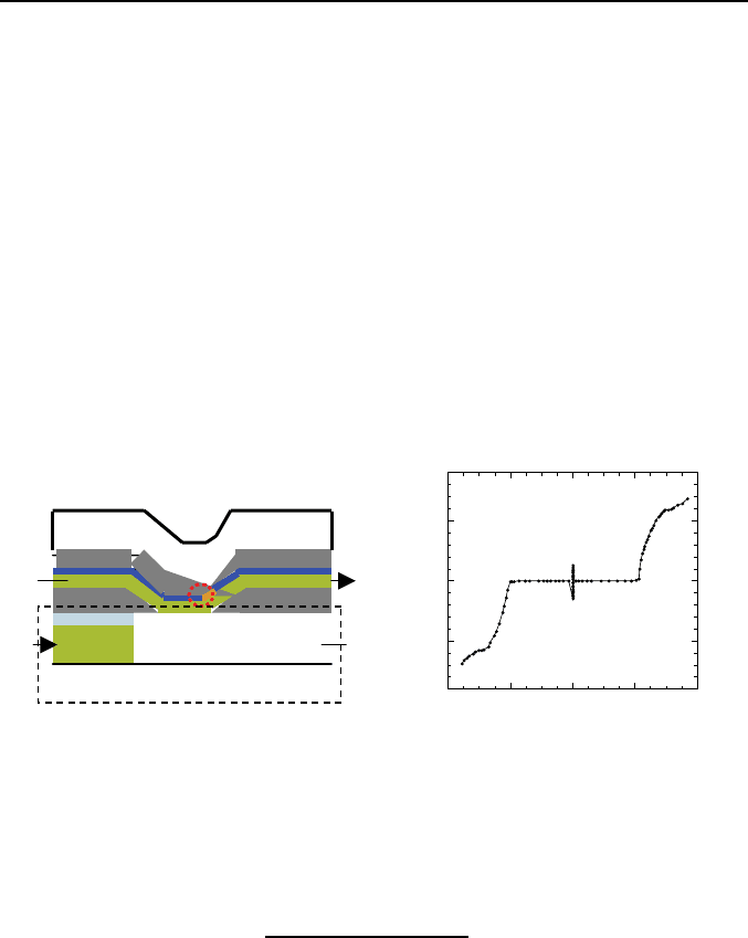
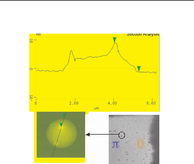
A detailed SEM and AFM analysis of devices where the fabrication
process has been stopped before closing the ferromagnetic junction with the
top Nb/Al bilayer, revealed the presence of inhomogeneities at the junction
window edges. SEM images (Fig. 5c) of the PdNi surface show such
inhomogeneities in the shape of black bubbles with 2-3
µ
m diameter.
Fig. 5b shows an AFM picture of the same surface, the line cut indicates the
direction along which a thickness profile has been measured (Fig. 5a).
Apart from inhomogeneities, the roughness is lower then 100 Å, while
picks as high as 500 Å develop on the top of the inhomogeneity itself. This
indicates that the PdNi layer is not continuous, thus inducing 0-coupling in
Superconducting/Ferromagnetic Nanostructures 235
such zones. Therefore, 0-junction and 0-
π
junctions are obtained with
PdNi layer thickness coresponding to 0-coupling and
π
- coupling
respectively.
Fig. 5. a) Roughness profile along the black line in (b). b) AFM picture of an
inhomogeneity at the window edge. c) SEM image of one window edge.
Results
Residual fields were screened by cryoperm and
µ
-metal shields. All
measurements showed comparable residual fields at 4.2 K of some tenths of
mG. Depending on the PdNi layer thickness, the ferromagnetic junction is
either 0 or
π
while a spontaneous half quantum vortex or antivortex is
expected only for
π
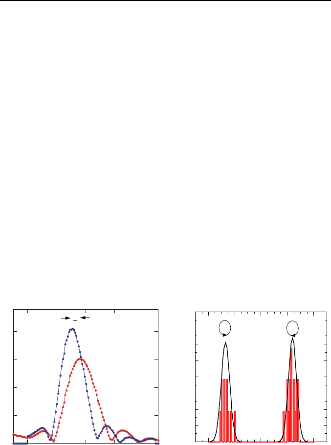
-coupling. In Fig. 6a we show the diffraction patterns
of a sample for a PdNi thickness of 100 Å corresponding to
π
-coupling at
T = 4.2 K (red data) and T = 2 K (blue data). The magnetic field
corresponding to a quantum flux is 300 mG. At T < T
cF
period reduction is
accompanied
by a
0
Φ /4 shift in the detector, as expected for a
spontaneous half quantum vortex in the ferromagnetic junction. Similar
period reductions have been observed for PdNi thickness of 40 Å and
200 Å
corresponding to zero coupling together with not shift in the
QuickTime™ et un
décompresseur TIFF (LZW)
sont requis pour visionner cette image.
π
a)
b) c)
236 M. Aprili, M. L. Della Rocca, T. Kontos
detector diffraction pattern [13]. The period reduction at the lowest
temperature (2 K) for all the samples was about 15%. This value results
from two competing effects: a smaller period is expected because of
screening in the ferromagnetic junction as shown in eq. 4, whereas the
decrease in the pénétration depth
λ
(T), at lower temperatures should
increase the modulation period. Note that no period reduction or diffraction
pattern shift are measured when the source and the detector are decoupled
with a thin insulating layer. This indicates that inductive coupling between
the two junctions is negligible.
Might an external residual field or the magnetic layer itself affect the
spontaneous supercurrents? In this regard it is important to stress that the
shift is always about
0
Φ /4 for
π
-coupling and zero for 0 coupling. Since
this depends neither on the residual field nor, for 0-coupling, on the
thickness of the ferromagnetic layer, any effect of the PdNi magnetic
moment on the amplitude of the spontaneous supercurrents seems to be
ruled out. Instead, the PdNi magnetic structure breaks the degeneracy of the
ground state and polarizes the supercurrents. As a consequence, the sign
shift is always the same below the Curie temperature (100 K), indicating
the same spontaneous current polarization. When cooling down from room
temperature to 2 K, the shift, while reproducible in magnitude, becomes
random in sign. This is shown in fig. 3b for 26 cool-downs of two different
junctions.
Fig. 6. a)
0
Φ
/4 shift in the diffraction pattern of the detector junction above
(T = 4.2 K, red dots) and below (T = 1.5 K, blue dots) the ferromagnetic junction
critical temperature, T
cf
. b) Statistics of the measured shift for 26 different cooling
down from room temperature. A positive shift correspond to half a quantum anti-
vortex, a negative shift to half a quantum vortex.
4
3
2
1
0
I (mA)
φ
4
0
B
d
PdNi = 100A
16
14
12
10
8
6
4
2
0
p
ercentage (%)
(a)
a) b)

Superconducting/Ferromagnetic Nanostructures 237
Conclusion
In conclusion, the strong enhancement of the Stoner factor at the
paramagnetic/ferromagnetic transition is measured by proximity effect
tunneling spectroscopy (PETS). Ferromagnetic Josephson
π
-junctions
behaves as classical spins resulting from spontaneous supercurrents which
are revealed by measuring the shift in the magnetic diffraction pattern of a
Josephson junction directly coupled to a 0-
π
junction.
Acknowledgments
This work has been supported by the ESF through the “
π
-shift” program.
We are indebted with E. Reinwald of the University of Regensburg for
performing the AFM analysis.
References
1. Wolf (1986) Principles of electron tunneling spectroscopy. Wiley and sons,
New York
2. For a review see Buzdin AI (2005). Rev Mod Phys 77:935
3. Bulaevskii LN, Kuzii VV, Sobyanin AA (1978). Solid State Comm 25:1053
4. Kontos T, Aprili M, Lesueur J, Dumoulin L (2004). Phys Rev Lett 93:137001
5. Andreev AF (1964). Sov Phys-J Exp Theor Phys 19:1228
6. Belzig W, Bruder C, Schön G (1996). Phys Rev B 53:5727
7. Daams JM, Mitrovic B, Carbotte JP (1981). Phys Rev Lett 46:65
8. Kontos T, Aprili M, Lesueur J, Grison X (2001). Phys Rev Lett 86:304
9. Golubov AA, Kupriyanov Yu (1988). J Low Temp Phys 70:823
10. Guichard W (2003). Ph.D. thesis, Université Joseph Fourier, Grenoble
11. Kontos T, Aprili M, Lesueur J, Genêt F, Stephanidis B, Boursier R (2002).
Phys Rev Lett 89:137007-1
12. Bauer A, Bentner J, Aprili M, Della Rocca ML, Reinwald M, Wegscheider
W, Strunk C (2004). Phys Rev Lett 92:217001
13. Della Rocca ML et al cond-mat/0501459
COHERENCE EFFECTS IN F/S AND N/F
NANOSTRUCTURES