Geckeler K.E., Nishide H. (Eds.) Advanced Nanomaterials
Подождите немного. Документ загружается.

21.2 Near-Field Raman Imaging Techniques 679
Raman spectra. Although extensive efforts have been devoted to fabricate fi ber tips
with a higher throughput, the throughput is still very low, especially for tips with
an aperture < 200 nm. In addition, the Raman signal is intrinsically weak (typically
less than 1 in 10
7
photons). A typical Raman spectrum takes several minutes to
record when using the conventional near - fi eld Raman method, which makes it
prohibitive to construct a Raman image in this way. For example, when Webster
et al . [7] used the aperture technique to study the stress distribution of a scratch
on a Si crystal wafer, a period of about 9 hours was required to obtain a Raman
image of 26 × 21 points.
An alternative approach to near - fi eld Raman microscopy is to use an aperture-
less confi guration (which is also known as tip - enhanced Raman scattering ; TERS )
[8 – 10] , employing a metal or metal - coated tip (see Figure 21.2 ). In this confi gura-
tion, the laser impinges on the apex of the metal tip, inducing a strong local electric
fi eld enhancement in the vicinity of the metal tip apex. In this case, the Raman
Figure 21.2 (a) Schematic diagram of
tip - enhanced Raman scattering in refl ection
geometry. The metal tip is brought to the
sample surface by tuning fork or cantilever.
The Raman signals can also be collected by
the focus lens instead of the collection lens;
(b) Magnifi ed view of the tip region. The
far - fi eld Raman signal comes from the whole
laser - illuminated area (a few μ m) and is
featureless, while the near - fi eld Raman signal
comes from only the tip region ( < 100 nm) and
carries information related to the device
features.

680 21 Near-Field Raman Imaging of Nanostructures and Devices
enhancement is a result of local fi eld enhancement by the tip, or increased polariz-
ability of the sample due to an interaction between the tip and sample, which is
similar to surface - enhanced Raman scattering. As the laser is delivered to the
sample surface by an objective lens rather than by a metal - coated fi ber tip, the low
optical throughput of conventional fi ber tips can be overcome. With a suitable
metal tip (usually Ag or Au), the Raman signal from the sample close to the tip
can be enhanced by several orders of magnitude.
Besides the higher overall Raman throughput, TERS has several other merits
over the apertureless confi guration:
1 . A higher spatial resolution : At least in principle, it is much easier to fabricate
a sharp tip than a small aperture. A spatial resolution < 10 nm has been achieved
using TERS.
2 . Fewer topographic artifacts : In aperture confi guration the tip is large, although
its aperture may be small; therefore, the tip cannot follow the sample surface
exactly. This is normally not a problem, and is less severe in TERS.
3 . A variety of potential tip materials : In addition to noble metals, silicon and
its oxides, nitrides, nanowires and nanotubes may represent good candidates
for tips.
4 . A wider spectral response range : Unlike the aperture technique, which usually
functions in the visible region due to a need to use optical fi bers to deliver the
laser, TERS can extend its applications to a much wider range, for example
from ultraviolet to IR.
Unfortunately, TERS also has some major disadvantages, the main challenge
being to obtain reproducible near - fi eld images. It is very diffi cult to achieve a
consistent near - fi eld enhancement in TERS, due to diffi culties in controlling the
geometry of the metal tip. The technique also encounters problems of wear and
tear, oxidation, and contamination of the tip apex (e.g., by carbon) that may have
severe adverse effects on the near - fi eld enhancement. Another problem is that the
laser spot, when focused on the tip apex, causes an intense background (far - fi eld
signal) that should be eliminated in order to achieve a better SNR [11, 12] . As a
result, TERS is rarely used for routine characterization.
A third approach, developed by the present authors ’ group, uses a dielectric
microsphere to focus the laser to a spot size that is smaller than the diffraction
limit. Besides being used as the excitation source for Raman spectroscopy, the
incident laser beam (linearly polarized Gaussian TEM00 mode) is also used to trap
the microsphere just above the sample surface, using the well - known “ optical
tweezers ” mechanism. In these experiments, the sample and polystyrene micro-
spheres (3 μ m diameter) were placed in a sample cell fi lled with deionized water.
One microsphere was trapped at the center of the laser beam and was in contact
with the surface of the sample during scanning. The experimental set - up is shown
schematically in Figure 21.3 a and b.
21.2 Near-Field Raman Imaging Techniques 681
Figure 21.3 (a) Schematic diagram of the near - fi eld Raman
microscope with microsphere; (b) Detailed description of the
sample cell: 1 = water immersion lens (60 × NA = 1.2 water
immersion), 2 = water, 3 = focused laser, 4 = cover glass,
5 = polystyrene microsphere (3 μ m), 6 = sample, 7 = sample
cell ’ (c) Typical Si
–
Si Raman intensity versus position with the
fi tted data to determine the laser spot size.

682 21 Near-Field Raman Imaging of Nanostructures and Devices
21.3
Visualization of Si
–
C Covalent Bonding of Single Carbon Nanotubes
Grown on Silicon Substrate
In this section, it is shown that Raman microscopy can be used to characterize
nanoscale samples, using Si
–
C bonding between the carbon nanotube s ( CNT s)
and the Si substrate as an example. Recently, CNTs have attracted a great deal of
interest on the basis of their extraordinary electrical, chemical, thermal, and
mechanical properties [13 – 15] , all of which make them promising materials for
applications in nanometer - scale electronics and devices. For example, a unique
property of CNTs is that they may be either metallic or semiconducting, depending
on their chirality and diameters [16] . The tuning of electrical properties of single
CNTs by inducing covalent bonding between the CNTs and the Si substrate has
been predicted [17 – 22] . Such direct integration of CNTs into well - developed silicon
technologies offers a new strategy of building nanoscale, or even single - molecule,
electronic devices by selectively forming covalent bonding between the CNTs and
the Si substrate.
Several groups have achieved Si – CNT bonding in ceramics with good mechani-
cal properties by annealing Si nanoparticles together with CNTs, which served as
a mechanical reinforcement [23] . The direct observation of Si
–
C covalent bonding
on single CNTs on Si substrate samples has not been reported, due partly to a lack
of suitable characterization techniques. However, it has been predicted that the
interaction between Si and the CNT results in a rich variety of changes in
the electronic structures of the CNT [19] . For example, when Miwa et al . studied
the single - walled CNT adsorbed onto partially and fully hydrogenated Si (001)
surfaces [19, 20] , it could be shown that the removal of a few H - atoms along the
adsorption sites would enhance the metallic character of the CNT. However, the
removal of all H - atoms would transform the CNT to the semiconducting state. By
using fi rst - principle calculations, Peng et al . were able to determine the binding
energies of CNTs adsorbed onto different sites on Si (001) surfaces [22] . In fact,
their results showed that the absorption sites at the surface trench for CNTs paral-
lel to the Si dimmer rows, and between Si dimers for CNTs perpendicular to the
Si dimer rows, were stable.
Such stability was also shown to depend heavily on the size (diameter) of the
CNTs. When preparing these Si – CNT devices the fi rst step is to fabricate Si – CNT
covalent bonding on a large scale. Irrespective of which technique is used to char-
acterize the sample, it must be capable of identifying those CNTs with Si
–
C bonds.
In these studies, a micro - Raman imaging technique [24] was used that was capable
of probing down to hundreds of nanometers, to investigate isolated single CNTs
and their interaction with the Si substrate. The CNTs were grown on a silicon
substrate at high temperature to achieve Si – CNT bonding, with Raman imaging
showing that some of the single CNTs were attached covalently to the silicon wafer
surface.
The CNTs were grown on the Si substrate using a thermal chemical vapor depo-
sition ( CVD ) technique, the substrate having been cleaned using trichloroethylene,

21.3 Visualization of Si
–
C Covalent Bonding of Single Carbon Nanotubes Grown 683
acetone, and ethanol in turn, by ultrasonic agitation. An ultrathin Fe fi lm to be
used as the catalyst was deposited in vacuo (10
− 5
Torr) by ion beam sputtering. The
substrates were pre - annealed at 850 ° C in a hydrogen - fi lled quartz tube furnace for
90 min. The CNTs were then grown at 1000 ° C for 20 min using methane, hydro-
gen, and argon with fl ow rates of 75, 20, and 100 sccm (standard cm
3
min
1
),
respectively. The sample was cooled below 300 ° C before being exposed to ambient
air, in order to avoid any damage caused by rapid cooling.
A JEOL JSM - 6700F scanning electron microscope was used to study the surface
morphology of samples and locations of interest for further Raman studies. The
Raman spectroscopy and imaging were carried out using a WITec CRM200 confo-
cal Raman system fi tted with an Olympus microscope objective lens (100 ×
NA = 9.5). A double - frequency Nd:YAG laser (532 nm, 100 mW laser; CNI Laser)
was used as the excitation source. The Raman scattered light was dispersed using
a grating (1800 grooves per millimeter), and detected using a thermoelectrically
cooled charge - coupled - device ( CCD ) cooled to − 64 ° C. A piezo - stage was used to
scan the sample for the Raman imaging. The spatial resolution of the Raman
imaging was approximately 250 nm.
The SEM image of the sample is shown in Figure 21.4 a. It can be seen that all
the CNTs were grown horizontally on the Si substrate, with random orientations.
The various diameters of the CNTs may be due to the different sizes of the Fe
catalyst. With assistance from markings on the Si substrate, Raman imaging was
performed in the same region shown in the SEM image. A careful analysis of the
Raman spectra in the Raman images revealed that the Raman spectra of the CNTs
shown in Figure 21.4 a could be indexed as two groups: (i) those consisting of only
normal CNT peaks; and (ii) those with additional peaks, which can be assigned to
Si
–
C bonds (this point is discussed later in the chapter). For simplicity, these two
types of spectra are referred to as CNT spectra and Si
–
C spectra, respectively.
Figure 21.4 b shows the typical Raman spectra of the two groups. The CNT spec-
trum shows only Raman bands of normal CNTs: the D band (1344 cm
− 1
), G band,
and 2D band (2681 cm
− 1
) [25] . The G band can be further identifi ed as the G – band
at 1570
− 1
and the G+ band at 1590 cm
− 1
. For certain CNTs (such as the CNT high-
lighted by the broken line in Figure 21.4 a), the Raman spectrum shows extra bands
belonging to Si
–
C bonds at approximately 1510 cm
− 1
(band A), 1692 cm
− 1
(band
B), 1921 cm
− 1
(band C), 1981 cm
− 1
(band D), 2392 cm
− 1
(band E), and 2620 cm
− 1
(band F). While several regions were tested in this study, it should be noted that
the extra bands (A – F) were observed only for certain CNTs, which suggested that
the Si
–
C bonds formed only for certain CNTs.
Raman imaging was performed in the sample region shown in Figure 21.4 a
with a scanning step size of 50 nm, and with the incident laser polarized in the
plane of the substrate. Raman images constructed using different peak intensities
are shown in Figure 21.5 a – d. Figure 21.5 a was generated by the G band (ca.
1580 cm
− 1
) intensity of the CNTs. Brighter regions represent CNTs, which show
an excellent correlation with those obtained using SEM. Images were also con-
structed using the intensity of the extra band A; the resultant image is shown in
Figure 21.5 b. The shape and position of the bright region matched perfectly the
684 21 Near-Field Raman Imaging of Nanostructures and Devices
CNT, emphasized by the dashed curve in the SEM image (Figure 21.4 a). Images
generated using bands B and F (not shown) exhibited near - identical patterns to
that of band A, clearly indicating that the three bands were all correlated to the
same CNT marked in the SEM image.
In order to confi rm that peaks A – F in Figure 21.4 b were indeed related to Si
–
C
covalent bonds, the Raman spectra were compared with those of bulk SiC, which
have been well studied [26, 27] . Bulk SiC has several polytypes, which can give rise
to the following fi rst - order Raman peaks: TA mode between 200 – 300 cm
− 1
, LA
mode at around 610 cm
− 1
, TO mode at around 790 cm
− 1
, and LO mode at near
970 cm
− 1
[28] . The TO mode at 790 cm
− 1
is by far the strongest Raman peak in all
polytypes, which is absent in the present sample (the reasons are given later). The
peak positions and relative intensities of the SiC second - order Raman bands varied
for different polytypes, with generally two characteristic bands: a broad band
Figure 21.4 (a) Scanning electron microscope image showing
the areas of interest. Raman bands belonging to Si
–
C bonds
can be detected on a carbon nanotube (CNT), as indicated by
the broken red line; (b) Comparison of Raman spectra
obtained on normal CNTs (black) and the special CNT (red).
The dashed lines represent the peak positions of the CNTs ’ D
band, G band, and 2D band.
between 1510 cm
− 1
and 1540 cm
− 1
, and a narrower band around 1710 cm
− 1
. Both
bands corresponded to multibands, resulting from the overlapping of different
overtone phonons of the SiC vibration [27, 29, 30] . As shown in Figure 21.4 b, both
band A (1510 cm
− 1
) and band B (1692 cm
− 1
) observed in these Raman spectra
showed a good agreement in shape and intensity with those two SiC characteristic
bands. The slight shift to lower wavenumbers ( Δ ω ∼ 10 cm
− 1
) may be due to the
small - size effect [31] . In addition, the weaker bands E and F also showed an agree-
ment with the broad band of SiC at 1930 cm
− 1
. As there have been no reports on
the Raman band of SiC above 2000 cm
− 1
, it was not possible to compare band F
with that of bulk SiC. However, the excellent agreement between the Raman image
using band F and those of band A and B showed that band F also belonged to the
Si
–
C bonds in this sample.
The fi rst - order Raman peak at 790 cm
− 1
is the strongest among all the Raman
peaks in all polytypes of SiC, but was absent from these experiments. This can be
explained by the substantial structural difference between the bulk SiC and
the present CNT/Si system, where all the Si
–
C covalent bonds were formed at
the Si – CNT interface. Such an unique an arrrangement deviates considerably
from that in the bulk SiC, where the Si
–
C covalent bonds are arranged in three
dimensions with a long - range order; in contrast, the bonds in the CNT/Si system
showed a long - range order in only one dimension – that is, along the long axis of
the CNTs.
Figure 21.5 Raman images constructed using peak intensity
of: (a) G band of CNTs and (b) Si
–
C band A at 1510 cm
− 1
.
The Raman images generated using bands at 1692 cm
− 1
and
2620 cm
− 1
are identical to those in panel (b). The green arrow
indicates the polarization of the incident laser. The blue
dotted lines serve as a guide to the eye, and show the
position and shape of the special CNT.
21.3 Visualization of Si–C Covalent Bonding of Single Carbon Nanotubes Grown 685

686 21 Near-Field Raman Imaging of Nanostructures and Devices
21.4
Near - Field Scanning R aman Microscopy Using TERS
The NSRM system used in these experiments consisted of a standard Nanonics
NSOM system and a Renishaw micro - Raman spectrometer. The Nanonics NSOM
system uses a bent optic fi ber tip (cantilevered tip), which makes the scanning
head very compact. The compact design allows the easy integration of the
spectrometer and NSOM by placing the scanning head under the microscope
objective of the Renishaw system [32] . An argon ion laser (488 nm line) is focused
onto the metal tip, which is made from tungsten wire through electrochemical
etching [similar to the method used in scanning tunneling microscopy ( STM ) tip
preparation], and then coated with silver through radiofrequency ( RF ) - sputtering
[33] .
The interaction between the tip and the laser enhances the local electrical fi eld
near the tip, which in turn enhances the Raman signal nearby. The same objective
lens collects the Raman signal in the backscattering geometry, which is then
directed into the Renishaw spectrometer by the coupling optics. In the confi gura-
tion described above, both the near - fi eld and far - fi eld Raman signals are collected.
In order to reduce the far - fi eld component, the laser beam must be focused tightly
to form a spot on the sample which is as small as possible. The collection effi ciency
of the optical system should also be high in order to obtain a good SNR, since the
Raman signal is intrinsically weak. These two aspects require a lens or objective
with a large numerical aperture ( NA ). In addition, the polarization direction and
incident angle have strong effects on near - fi eld enhancement, and these should
be tuned carefully. The polarization direction is tuned by a λ /2 plate, which is
placed just before the laser and adjusted to be perpendicular to the beam. As
shown by computer simulations, the near - fi eld enhancement is not maximum
when the laser beam is parallel to the tip axis. To maximize the near - fi eld enhance-
ment, two approaches can be used: the fi rst approach is to set the tip oblique to
the sample and use backscattering geometry; the second is to use a perpendicular
tip and an oblique incident laser.
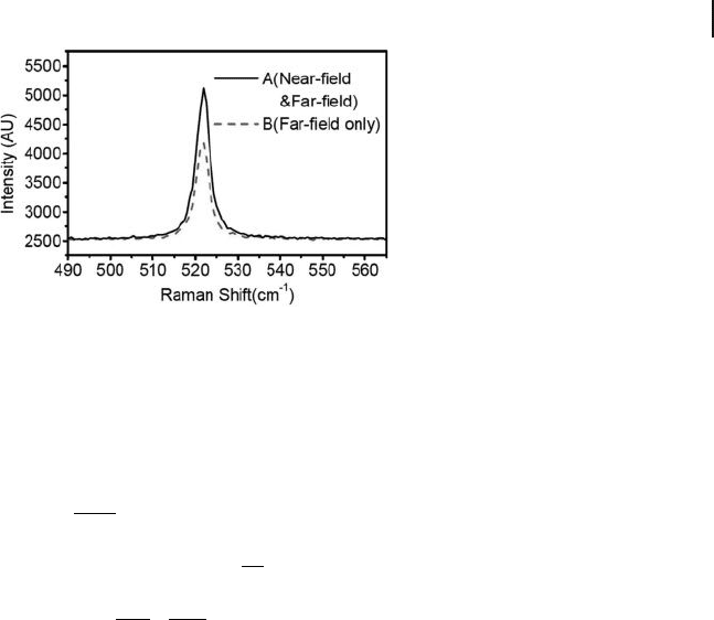
To observe the near - fi eld enhancement, an experiment on single crystal
silicon was performed. For this, the single crystal silicon was placed on the
piezo scanning stage of the NSOM system, and the silicon Raman peak at
520 cm
− 1
recorded for two tip positions: (i) with the tip “ touching ” the silicon
surface to record the Raman spectrum, which includes both the near - fi led
and far - fi eld components; and (ii) with the tip lifted from the surface so as to
record the far - fi eld Raman spectrum. These are shown as spectra in Figure 21.6 a
and b, respectively. The near - fi eld component is approximately 50% of the far - fi eld
signal.
It should be noted that the near - fi eld Raman signal comes from a small
region on the sample, while the far - fi eld signal comes from a much larger volume
(about 2.5 μ m in diameter for our instrumental setup and the laser penetration
of Si is about 0.5 μ m). Assuming that the diameter of the metal tip is several
tens nanometers, say 70 nm, and the near - fi eld enhancement occurs at a depth
21.4 Near-Field Scanning Raman Microscopy Using TERS 687
Figure 21.6 The silicon Raman spectra with the tip “ touching ”
the sample surface (spectrum A) and the tip withdrawn
(spectrum B).
of 20 nm of the Si sample. The far - fi eld signal derives from a volume of
V
far
=
()
×π
2500
2
500
2
3
nm , while the near - fi eld signal is derived from a much
smaller volume
V
near
=
()
×π
70
2
20
2
3
nm
. The enhancement factor can be
estimated as
I
I
V
V
near
far
far
near
× , where I
near
= 0.35 I and I
far
= (1 − 0.35) I are the measured
near - and far - fi eld Raman intensities, respectively. Such a simple estimation shows
that the near - fi eld enhancement factor is more than 10
4
. In another experiment,
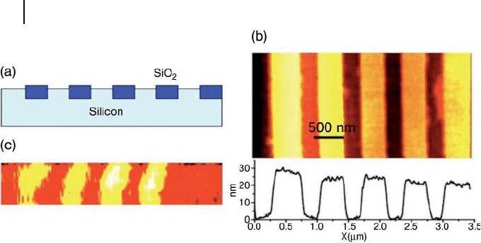
the improvement in spatial resolution was demonstrated by using a featured
sample: a silicon device, which consists of SiO
2
lines of 380 nm width, with 300 nm
separations. The SiO
2
lines were 30 nm higher than the silicon substrate ( Figure
21.7 a). By comparing the width of the SiO
2
strips in the AFM profi le and the real
width (380 nm), the topographic spatial resolution of the set - up was derived as
34 nm (Figure 21.7 b). Raman mapping (128 × 20 points) was performed on a strip,
and the Raman image constructed using the Raman peak intensity, as shown in
Figure 21.7 c. The Raman spectra were collected with a 1 s integration time. In this
experiment, the Raman spectrum contained both far - fi eld and near - fi eld compo-
nents when the tip was on a Si - single crystal, but had only the far - fi eld component
when the tip was on SiO
2
, where the SiO
2
prevented the tip from coming close
enough to the Si to excite its near - fi eld Raman signal. Hence, the intensity varia-
tion of the Si Raman peak represented the near - fi eld contribution, while the far -
fi eld contributed a constant background. The Raman intensity image shown in
Figure 21.7 c has a clear correlation with the Si device, as might be expected. This
was the fi rst two - dimensional ( 2 - D ) near - fi eld Raman image of a real nanometer -
sized device. The 1 s integration time required to record a good quality Raman
spectrum is short enough to make NSRM a useful technique for imaging
purposes. It should be noted that the SiO
2
lines in the NSRM image are
not straight, due to hysteresis and creep of the piezoelectric scanner, which is
688 21 Near-Field Raman Imaging of Nanostructures and Devices
calibrated and linearized in normal AFM scanning. In Raman mapping, however,
the scanning rate is much lower than that in normal AFM scanning, as the
scanner must remain at each point for several seconds while the spectrometer
records the Raman spectrum. Thus, the creep will become more obvious during
the mapping process.
21.5
Near - Field R aman Imaging Using Optically Trapped
Dielectric Microsphere
Recently, a new approach to near - fi eld imaging has been developed, whereby the
laser is focused to a spot size which is smaller than diffraction limit, by using a
dielectric microsphere. In addition to being used as the excitation source for Raman
spectroscopy, the incident laser beam (linearly polarized Gaussian TEM00 mode)
is also used to trap the microsphere just above the sample surface, through the
well - known “ optical tweezers ” mechanism [34, 35] . Simulation studies have shown
that subdiffraction - limited focusing can be achieved when the diameter of the
dielectric microsphere is comparable to the wavelength of laser [36, 37] . In the
experiments, the sample and polystyrene microspheres (3 μ m diameter) in solution
were placed in a sample cell fi lled with deionized water. One microsphere was
trapped at the center of the laser beam, and was in contact with the surface of the
sample during scanning. The schematic diagram of the experimental set - up is
shown in Figure 21.3 a. The near - fi eld Raman microscopy set - up with polystyrene
microsphere is based on the WITec CRM200 confocal Raman microscopy system
Figure 21.7 (a) Schematic cross - sectional diagram of the Si
device sample; (b) Atomic force microscopy image of the Si
device sample; (c) Raman intensity image of the Si device
sample.