Geckeler K.E., Nishide H. (Eds.) Advanced Nanomaterials
Подождите немного. Документ загружается.

1.2 Block Copolymers as Lithographic Materials 25
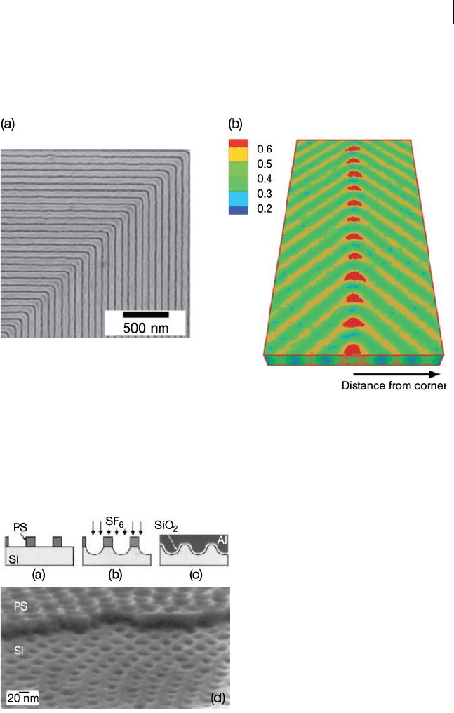
Figure 1.11 (a) A top - down SEM image of
angled lamellae in a ternary PS - b - PMMA/PS/
PMMA blend. The chemical surface pattern is
fabricated with a 70 nm line spacing to match
the natural period of the copolymer;
(b) Theoretical concentration map of the
distribution of the homopolymers on the
surface. The homopolymers concentrate and
swell the polymer at the bend area of the
patterns to prevent the formation of defects.
Reprinted with permission from Ref. [131] ;
© 2006, American Association for the
Advancement of Science.
the fi rst to demonstrate the industrial feasibility of this technology. After optimiza-
tion of the process window for maximum ordering of perpendicular - oriented
nanodomains [132, 133] , Black ’ s group demonstrated the successful fabrication of
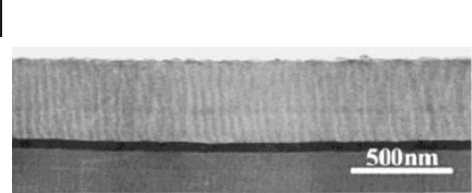
metal - oxide - silicon ( MOS ) capacitors (Figure 1.12 ) [133 – 135] , multinanowire
Figure 1.12 The process fl ow for MOS
capacitors. (a) Polymer template formation on
silicon surface; (b) RIE pattern transfer of PS
template into silicon, followed by removal of
the PS matrix; (c) SiO
2
growth followed by top
A1 gate electrode deposition; (d) SEM image
at a 70 ° tilt after RIE etch. The remaining PS
template is shown at the top. At the bottom,
the nanoscale hexagonal array has been
transferred into a Si counter electrode.
Reprinted with permission from Ref. [134] ;
© 2006, American Institute of Physics.
26 1 Phase-Selective Chemistry in Block Copolymer Systems
silicon fi eld effect transistors [136] , and FLASH memory devices [137] . The crea-
tion of high - aspect ratio patterns has always been problematic due to the diffi culty
of achieving a single microdomain orientation in thick BCP fi lms. In this area,
Thurn - Albrecht and coworkers reported that the application of a strong electric
fi eld, in combination with thermal annealing, creates 500 nm - long, vertically ori-
ented PMMA cylinders that physically connect to the substrate, as shown in Figure
1.13 . After PMMA removal, the underlying conducting substrate was used for the
subsequent deposition of copper into the holes to form a matrix of continuous
nanowires [90] .
Asakawa and coworkers from the Toshiba Corporation were the fi rst to pattern
magnetic media for hard disk applications, by using a PS - b - PMMA template. In
these investigations, the group took advantage of the large difference in etch resist-
ance between the aromatic and acrylic polymer to produce the BCP template using
dry etching techniques [108, 109] . Spiral - shaped circumferential grooves were
imprinted into a hard - baked photoresist using a nickel master plate. The spherical
PMMA microdomains then aligned within the walls of the grooves, and the
PMMA was preferentially etched by oxygen plasma to create holes which con-
nected to an underlying magnetic cobalt platinum fi lm. The size of these holes
could be adjusted by changing the molecular weight of the PS - b - PMMA. The holes
were then fi lled with etch - resistant spin - on - glass, which acted as a mask while the
remaining PS polymer and the underlying magnetic media were patterned by ion
milling. After removal of the spin - on glass, the disk featured magnetic nanodots
arranged in a spiral pattern.
PS - b - PMMA has proved to be an excellent system to perform studies on the
ability of BCPs to act as nanolithographic stencils, although doubts persist regard-
ing its potential to enter into industrial, high - volume production. For example, as
noted previously, crosslinking the matrix phase of the BCP is necessary to prevent
pore collapse during the rough pattern transfer and etching step. PS, however,
cannot be crosslinked (or patterned) effi ciently upon exposure to UV light. A
combination of different photochemical processes, such as random chain scission,
oxidative coupling and crosslinking, all occur at the same time during UV expo-
Figure 1.13 Cross - sectional transmission
electron microscopy image obtained from
a PS - b - PMMA fi lm (800 nm) annealed in an
electric fi eld of 25 V μ m
− 1
. The block
copolymer fi lm is lying on top of a dark
Au - fi lm, which was used as the lower
electrode. The upper electrode has been
removed. Cylinders oriented normal to the
substrate pass all the way through the
sample. Reprinted with permission from
Ref. [90] ; © 2006, Wiley - VCH.

1.2 Block Copolymers as Lithographic Materials 27
sure, as shown previously in Scheme 1.8 . Several groups have taken steps to
correct this problem, with Hawker and coworkers [103] having randomly copoly-
merized thermally crosslinkable benzocyclobutene ( BCB ) groups with polystyrene
(PS - ran - BCB). The degree of crosslinking can be tuned by increasing the amount
of the BCB in the random copolymer. Microdomain ordering was induced by
thermally annealing the matrix at 160 ° C. Raising the temperature to 220 ° C caused
the matrix to be crosslinked, and the PMMA was exposed and developed in the
normal manner.
Poly(Styrene - b lock - Lactic Acid) Poly(styrene - block - lactic acid) (PS - b - PLA) is another
copolymer that has been developed as a nanolithographic template. To synthesize
this polymer, hydroxyl - terminated PS (prepared through anionic polymerization)
was treated with triethylaluminum to form the corresponding aluminum alkoxide
macroinitiator. This species was able to effi ciently polymerize d , l - lactide through
a ring - opening process [118] . The advantage of using this BCP as a nanolitho-
graphic template is that PLA undergoes main - chain cleavage simply by soaking it
in an aqueous methanol mixture containing sodium hydroxide at 65 ° C. The PS
matrix is not affected at all by this treatment. Zalusky and coworkers have also
published a complete phase diagram and characterization of PS - b - PLA [119] . Leis-
ton - Balanger and coworkers used the benzocyclobutene crosslinking strategy
explained in Section 1.2.2.1.2 but with PLA as the minority component, thus
eliminating the photoprocessing step [138] . The group noted that, if a thermally
degradable minority component were to be used, then a robust nanoporous tem-
plate could be produced by using a completely thermal process.
Poly(Styrene - b lock - Ferrocenyldimethylsilane) BCPs containing organometallic ele-
ments can also function very well as nanolithographic etch masks, as shown by
the studies of Thomas and coworkers [113, 114, 139] . Thomas ’ group was able to
synthesize a BCP of poly(styrene - block - ferrocenyldimethylsilane) ( PS - b - PFS ) that
organized into lamellar and cylindrical microdomains by using an anionic ring -
opening polymerization. The PFS block contained elemental iron and silicon,
which made it highly resistant to dry - etching processes due to the creation of iron
and silicon oxides during oxygen etching. The resulting etching ratio between PS
and PFS was estimated to be as high as 50:1. Thus, by etching through the poly-
styrene, the BCP patterns were transferred into the underlying substrate in only
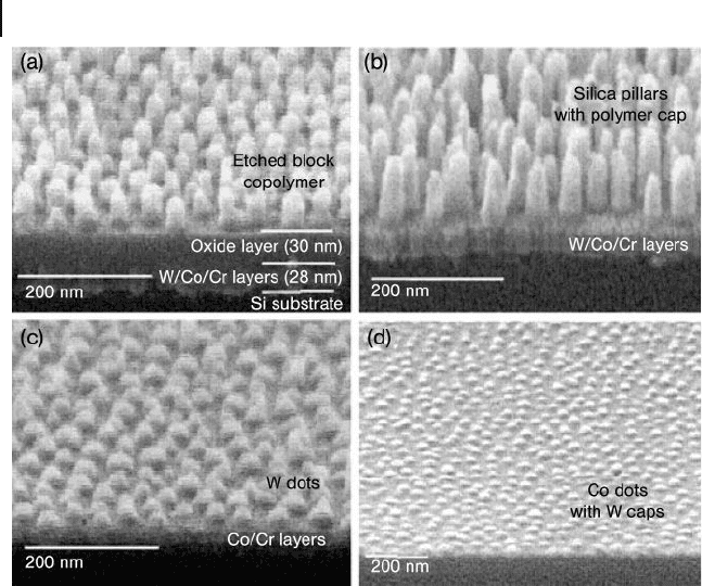
one step. By using this polymer as a masking layer, Thomas et al . further demon-
strated that an array of cobalt single - domain magnetic particles could be created
through a tri - level etching strategy (Figure 1.14 ). Moreover, the magnetic proper-
ties and thermal stability of the dots could be tuned simply by changing the
copolymer composition and etch depth into the cobalt [123, 140] .
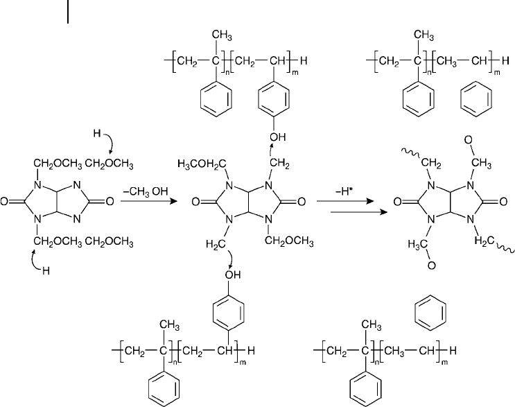
Poly( α - Methylstyrene – b lock - Hydroxystyrene) Studies conducted by the present
authors ’ group have focused on poly( α - methylstyrene - block - hydroxystyrene) (P α -
MS - b - HOST) that allows not only an effi cient crosslinking of the hydroxystyrene
matrix phase but also the ability to lithographically pattern the nanoporous tem-
28 1 Phase-Selective Chemistry in Block Copolymer Systems
plates on select areas of the wafer [116, 117] . In these studies, traditional chemical
amplifi cation strategies [141] , which have been recognized among the photoresist
community for over 20 years, were used in combination with BCP lithography.
An overview of the processing scheme is presented in Figure 1.15 . The key to
chemical amplifi cation strategies is the use of cationic catalysts known as pho-
toacid generator s ( PAG s); these produce a strong acid when exposed to DUV
radiation (248 and 193 nm). Trifl ic acid generated by the PAG molecule (tri -
phenylsulfonium trifl ate) was used to catalyze a condensation reaction [142]
between the hydroxyl groups of the poly(hydroxystyrene) and a crosslinking
species tetramethoxymethyl glycoluril ( TMMGU ; Powderlink 1174) to produce,
in turn, a highly crosslinked network of the matrix phase (Scheme 1.9 ). The areas
of the wafer where nanoporous templates are not needed are washed away with
a solvent development step. The crosslinked regions of PHOST contained stand-
ing, 20 nm - diameter cylinders of poly( α - methylstyrene), a polymer that can be
depolymerized and removed from the matrix with additional UV irradiation, heat,
Figure 1.14 Tilted SEM images of the
intermediate stages of lithographic
processing. (a) An O
2
- RIE - treated block
copolymer thin fi lm on a multilayer of silica,
the metallic fi lms, and the silicon substrate;
(b) Pillars of silicon oxide capped with
oxidized PFS after CHF
3
- RIE; (c) Patterned
tungsten fi lm using CF
4
+ O
2
- RIE on top of
a cobalt layer after removing the silica and
residual polymer cap; (d) W - capped cobalt
dot array produced by ion beam etching (note
the different magnifi cation). Reprinted with
permission from Ref. [123] ; © 2006,
Wiley - VCH.
1.2 Block Copolymers as Lithographic Materials 29
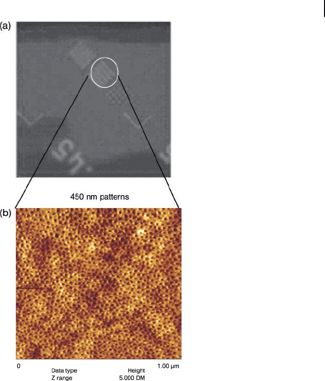
and high vacuum. Thus, by using standard lithography procedures, it was pos-
sible to generate 450 nm resolution patterns of crosslinked PHOST containing
20 nm nanoporous substructures, as shown in Figure 1.16 . Further processing
of this polymer in order to maximize the degree of long - range ordering is cur-
rently under way [143] . It is believed that this combination of traditional “ top -
down ” positive - and negative - tone lithography techniques, in combination with
the power of “ bottom - up ” BCP self - assembly, holds much promise for the future
of lithography.
1.2.3
Multilevel Resist Strategies Using Block Copolymers
The constant drive for smaller and smaller circuit device features with higher
aspect ratios and more complex substrate topographies has caused many photo-
lithographic engineers to rethink traditional single - level resist - processing strate-
gies. As sub - 100 nm feature sizes become the norm, artifacts arising from the
lithographic process that were recently deemed insignifi cant have now become
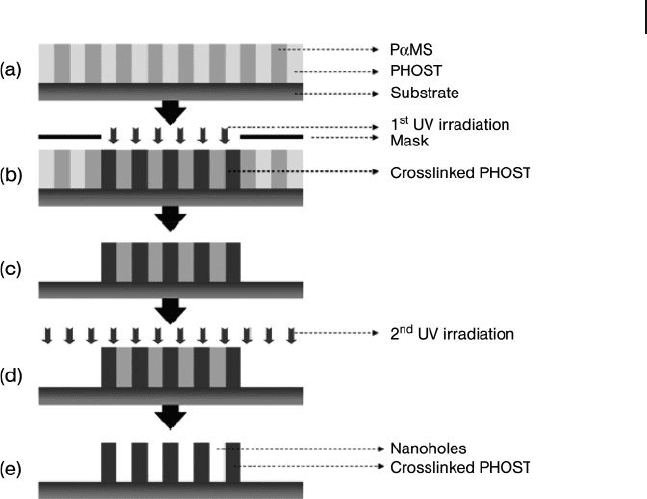
Figure 1.15 Novel nanofabrication process of
obtaining spatially controlled nanopores.
(a) Spin - coating of a P α MS - b - PHOST/PAG
mixture onto a silicon wafer to form vertical
cylinders of P α MS in the PHOST matrix;
(b) Irradiate using a 248 nm stepper with a
photomask and bake; (c) Develop with a
mixed solvent to form micron - sized patterns
on top of the substrate; (d) Irradiate using a
365 nm lamp under vacuum; (e) Form
patterns with nanoporous channels. Reprinted
with permission from Ref. [117] ; © 2006,
American Chemical Society.
30 1 Phase-Selective Chemistry in Block Copolymer Systems
major problems. One such artifact that limits resolution is the creation of the
“ standing wave effects ” which occur when UV light refl ects off the substrate
surface after passing through the resist [73] . As a result, multilevel resist chemis-
tries have been developed to incorporate polymeric planarizing layers to eliminate
substrate topography variability and anti - refl ection coatings to eliminate standing -
wave patterns in photoresists. Commonly used multilevel strategies employ a
photoresist imaging layer on top of the planarization layer. The resist used for the
imaging layer is designed to provide high sensitivity to UV light exposure by pro-
viding a large number of photosensitive functional groups, and must be highly
etch - resistant to the extremely harsh conditions imposed by the oxygen reactive
ion - etching step. Organosilicon - containing polymers have been demonstrated to
be excellent candidates as etch - resistant photoresists, due to their ability to form
a protective SiO
2
ceramic upon exposure to oxygen plasma, as shown by Taylor
and Wolf [144, 145] . The only disadvantage of these polymers is that their bulky
side groups result in very low T
g
- values, which make them susceptible to viscous
fl ow and excess swelling during the development step. Photoresist engineers typi-
cally counter the problem of low T
g
values by randomly copolymerizing the etch
Scheme 1.9 Proposed crosslinking mechanism of P α MS - b -
PHOST with TMMGU. After Roschert, H., Dammel, R., Eckes,
C. et al. (1992), Proc. SPIE - Int. Soc. Opt. Eng ., 1672 , 157.
1.2 Block Copolymers as Lithographic Materials 31
resistant, low - T
g
polymer with a photosensitive polymer that also has a high T
g
.
The copolymerization of the two monomers is necessary to avoid the inevitable
macrophase separation that results when two homopolymers are mixed together.
This composite style approach thereby simultaneously satisfi es the requirements
for high etch resistance, high sensitivity and high T
g
, resulting in the best - per-
forming photoresists.
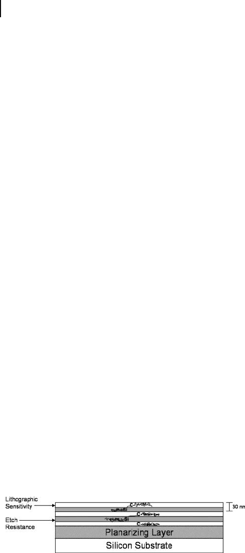
BCPs seem to be a perfect fi t for multilevel resist chemistries, due to their
ability to segregate into chemically distinct levels and their intrinsic ability to avoid
Figure 1.16 Atomic force microscopy height images showing:
(a) the 450 nm photopattern produced through the
crosslinking of the PHOST matrix; and (b) the 20 nm - diameter
porous substructure generated after removal of the
α - methylstyrene block.
32 1 Phase-Selective Chemistry in Block Copolymer Systems
macrophase separation. It is well known that a BCP fi lm will self - assemble such
that the lower surface energy block is presented at the polymer/air interface. This
principle can in turn be used to design layered systems of different functionality,
as will be seen in the creation of semi - fl uorinated BCPs for low - surface energy
applications (see Section 1.6.1 ). For example, to create the imaging layer a polymer
containing photosensitive tert - butyl functional groups may be used along with an
etch - resistant organosilicon polymer (Figure 1.17 ). Conveniently, the tert - butyl
groups contain three low - energy methyl groups that drive the segregation of the
photoactive compound to the surface, where it is most effectively exposed to UV
light. The surface - segregating properties are not limited to the tert - butyl group,
however; many other protecting groups could be used. Moreover, the functional,
chemically distinct polymers used in photoresists will exist in a microphase - sepa-
rated state if they are incorporated into a BCP. The microdomains form with
diameters within one radius of gyration of the polymer chain, which usually is
about 5 – 30 nm. Therefore, a patterned lithographic feature on the BCP photoresist,
currently approximately 100 – 200 nm, will contain numerous domains of the pho-
tosensitive and etch - resistant functionalities incorporated within it to ensure
optimal performance of the photoresist.
The microphase separation of BCPs also means that each one of the polymer
chains is confi ned to its own respective domain, and can be thought of as being
artifi cially crosslinked. Thus, in negative - tone resists, less UV light is required to
cause the polymers to become insoluble compared to a homopolymer of a similar
molecular weight. BCPs have also been shown to be twice as sensitive to nonphase -
separated random copolymers using the same monomer units and molecular
weight, due to this confi nement effect [146] . Confi nement might also mean that
the PAG moieties used in these resists might be clustering selectively inside one
of the microdomains, and this effect might be magnifi ed if the PAG is miscible
in only one of the BCP microdomains [147] . Moreover, if the usually hydrophilic
photoacid segregates inside the block containing the acid - labile functional groups,
the effective concentration of the acid will be increased, which means that a higher
percentage of the protecting groups will be converted to base - soluble – OH groups.
Hartney and coworkers [148] developed the fi rst application for BCPs as bi - level
e - beam resists in 1985, when they prepared a BCP of poly(chloromethylstyrene)
for sensitivity and high T
g
, and poly(dimethylsiloxane) ( PDMS ) that forms etch -
resistant silicon oxide upon exposure to oxygen plasma and has a low T
g
. Bowden
et al . subsequently prepared a PDMS BCP grafted to PMMA that acted as a neg-
ative - tone resist [149, 150] , while Jurek et al . created a novalac oligo - PDMS resist
Figure 1.17 Multilevel resist strategy using block copolymers. Adapted from Ref. [148] .

1.2 Block Copolymers as Lithographic Materials 33
which showed resolutions of 500 nm and etch rates which were 36 - fold slower than
hard - baked novalac [151] . Gabor and coworkers attached a PDMS graft to the
double bonds of an isoprene block in a styrene - block - isoprene BCP to create a
negative - tone resist. In this way, Gabor et al . achieved line - space patterns of
200 nm using e - beam lithography, and demonstrated oxygen etching rates which
were 42 - fold slower than for polyimide [152] . Other resists which have incorpo-
rated PDMS for etch resistance in both block and graft copolymer architectures
have also been reviewed [153] .
Gabor and coworkers also prepared block and random copolymers of poly( tert -
butyl methacrylate) and a silicon - containing methacrylate (poly(3 - methacryloxy)
propyl pentadimethyldisiloxane) (Figure 1.18 ) via group transfer polymerization
for applications in 193 nm photolithography [154] . The BCP architecture allowed
Gabor ’ s group to incorporate a larger amount of the hydrophobic siloxane com-
ponent for a high - oxygen RIE resistance, while maintaining solubility in an
aqueous base developer. In fact, the BCPs were found to have a better development
behavior in aqueous base than their random copolymer counterparts (Figure 1.19 ).
Gabor et al . hypothesized that the exposed polymeric regions formed micelles in
the aqueous base developer, with the silicon - containing block forming the core
and the soluble methacrylic acid group forming the corona. In contrast, random
copolymers would not have the ability to form these micellar structures; that is,
the entire copolymer would need to be soluble in order for development to occur.
However, the development behavior of these BCPs was far from perfect, presum-
ably due to segregation of the PAG away from the surface of the fi lm. Although
their performance does not exceed commonly used industrial photoresists, the
concept of using BCP architectures for multilevel photoresists is enticing, and
there may be much more to learn from these types of systems.
Figure 1.18 Block copolymer designed as a multilevel
photoresist: t - butyl methacrylate ( t - BMA ) - block - 3 -
methacryloxy - propylpentamethyldisoloxane (SiMA).

34 1 Phase-Selective Chemistry in Block Copolymer Systems
1.3
Nanoporous Monoliths Using Block Copolymers
1.3.1
Structure Direction Using Block Copolymer Scaffolds
Besides the potential uses of BCPs as lithographic materials, their inherent micro-
phase separation and chemical dissimilarity of the blocks also leads to other
applications. For example, BCPs can serve as structure - directing agents for the
formation of mesoporous monolithic materials through phase - selective chemistry.
Monolithic nanoporous structures have a large surface : volume ratio, which means
that there is a large amount of functionalizable surface area within a small volume
of material. In one of the pioneering efforts in this area, Hashimoto and coworkers
created a bicontinuous morphology with poly(styrene - block - isoprene) and selec-
tively removed the minority isoprene domain with ozonolysis [115] . The group
showed that coating the bulk structure with nickel metal does not completely block
the nanopores. Rather, metal catalysts such as nickel are known for their ability
to adsorb and split H
2
molecules for large - scale industrial reactions such as hydro-
genation. The high surface : volume ratio of porous bicontinuous BCP morpholo-
gies make them excellent candidates for catalytic applications; indeed, one day they
may even be used to make your margarine!
The BCPs used as structure - directing “ scaffolds ” to create mesoporous silicate
structures could also be used as dielectric materials. Silicon dioxide (SiO
2
) is typi-
cally used as a dielectric material to reduce undesired capacitive coupling between
neighboring elements of an integrated circuit, due to its low dielectric constant ( k )
Figure 1.19 (a) A block copolymer photoresist
poly( tert - butyl methacrylate - block - [3 -
(methacryloxy)propyl]pentamethyldisiloxane)
with 10.0 wt% silicon, formulated with 5 wt%
PAG. An exposure dose of 2 mJ cm
− 2
was
used, and the resist was developed for 20 s in
a mixture of 27% 0.21 N
tetramethylammonium hydroxide ( TMAH )
and 73% iso - propyl alcohol; (b) Random
copolymer with 9.7 wt% silicon, formulated
with 5 wt% PAG, after 1.2 μ m features are
exposed to 19 mJ cm
− 2
and developed using
the same conditions. While the random
copolymer is insoluble, pinholes form during
development and are thought to originate
from phase - separated acid, which is removed
by the developer. Reprinted with permission
from Ref. [154] ; © 2006, American Chemical
Society.