Geckeler K.E., Nishide H. (Eds.) Advanced Nanomaterials
Подождите немного. Документ загружается.


1.2 Block Copolymers as Lithographic Materials 15
polymers feature delicate protecting groups that may be unsuitable for the highly
reactive initiators used in living polymerizations. Polymer - analogous reactions
can create copolymers that could not have been synthesized within a living polym-
erization. These modifi cations are carried out on previously synthesized, or “ pre-
cursor ” BCPs such as poly(styrene - block - isoprene) with known molecular weights
and narrow molecular weight distributions. Chemical transformation of the pre-
cursor polymer can be carried out selectively on individual blocks, on the entire
copolymer, or on each block in sequence. Here, careful selection of the reaction
conditions is vital to avoid any harmful side reactions such as degradation or
crosslinking of the original polymer. If carried out successfully, the degree of
polymerization, molecular weight distribution, and main chain architecture of
the precursor polymer will remain the same, but the solubility and physical prop-
erties of the polymer may be altered completely. Examples of polymer analogous
reactions include hydrogenation [60] , epoxidation [61] , hydrolysis [62] , sulfonation
[63] , hydroboration/oxidation [64, 65] , quaternization [66] , hydrosilylation [67] , and
chloro/bromomethylation [68, 69] . Further details for each of these reactions is
also available [71] .
In this section, we have set the foundation for understanding how the chemistry
of block copolymeric materials relates to the physics of their unique self - assem-
bling properties. In the remainder of the chapter, it will become clear how these
novel chemical strategies are used to effect practical physical applications.
1.2
Block Copolymers as Lithographic Materials
1.2.1
Introduction to Lithography
A modern integrated circuit is a complex, 3 - D network of patterned wires, vias,
insulators, and conductors. In order to transfer these patterns onto the silicon
substrate it is fi rst necessary to write the pattern, and for this the technique of
photolithography is used, in which radiation - sensitive polymers play an integral
role. Standard photolithography consists of essentially two steps: (i) writing of the
pattern into a radiation - sensitive polymer thin fi lm (resist); and (ii) transferring
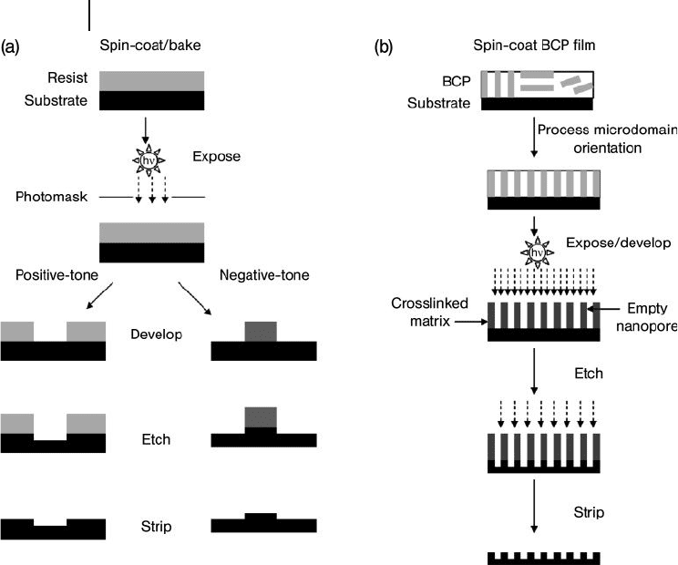
the pattern by etching into the underlying substrate [72] . A schematic of the tra-
ditional lithographic process is shown in Figure 1.7 a. As photolithography and its
associated technologies will become a recurring theme in this chapter, a brief
primer on the subject will be useful at this point.
During the exposure process of a polymeric photoresist, UV radiation passes
through a quartz photo mask that only allows a particular pattern of radiation to
pass through and strike a thin fi lm of photoresist. A chemical change is effected
in the exposed regions of the polymer, which allows its subsequent development
in a solvent, similar to the way in which photographic fi lm is exposed and devel-
oped in a darkroom. The mechanism of the chemical change involves the forma-
16 1 Phase-Selective Chemistry in Block Copolymer Systems
tion, rearrangement or breaking of bonds within the polymer chain. A resist ’ s
sensitivity is a measure of how effi ciently it responds to a given amount of radia-
tion, and might be compared to the ASA or ISO rating of a photographic fi lm. A
resist with a higher sensitivity will allow a satisfactory image to be produced for a
smaller absorbed dose of radiation. The resolution of a photoresist is the size of the
smallest structure that can be cleanly resolved after pattern development using
standard microscopy techniques. This structure will then be used to effi ciently
pattern into the underlying substrate, assuming that the photoresist has suffi cient
etch resistance to withstand the harsh pattern transfer step. In this step, the pat-
terned resist must withstand high - energy plasma sources that are designed to etch
into silicon wafers. Polymers containing more carbon have stronger dry - etch
resistance than those with lower amounts of carbon, whilst polymers containing
high amounts of oxygen are etched easily. Even etch - resistant polymers may lose
Figure 1.7 (a) Schematic of a traditional photolithography
using positive - tone or negative - tone resist chemistry.
(b) Schematic of block copolymer lithography, using a
combination of positive - tone and negative - tone resist
chemistry.

1.2 Block Copolymers as Lithographic Materials 17
a small amount of material during the etching step, but maintaining the structure
of the pattern is important for high resolution. If less than a ± 10% change in the
fi nest feature size of the polymer is etched into the substrate, the pattern transfer
step is deemed successful [73] . This presents a huge challenge for the resist
designer, who must tune the chemical components of the photoresist to satisfy
two diametrically opposed requirements: to design a resist that is very responsive
to ultraviolet radiation, but which, after the initial exposure, becomes highly resist-
ant to the specifi c type of radiation and heat involved in the pattern transfer step.
This is often achieved through the copolymerization of more than one type of
monomer, each having its own functionality in the photoresist.
The realm of photolithography is split into two families of chemistry, based on
the different physical properties possible for the exposed photoresist:
• Positive - tone resist chemistry refers to a photoresist that becomes more soluble
after exposure to UV light. This can happen because of chemical deprotection,
bond rearrangement, or chain - scission mechanisms.
• Negative - tone resist chemistry refers to a photoresist that becomes less soluble
through the formation of crosslinked networks after exposure to UV light.
In this chapter, we will highlight the many approaches that have been used for
one or both of these types of chemistries, in order to fabricate functional nanos-
cale - sized structures using BCPs.
1.2.2
Block Copolymers as Nanolithographic Templates
The lithography community has been extremely successful in its ability to pack
progressively more circuit elements into a chip, as governed by the benchmark
pace fi rst predicted by Gordon Moore in 1989, which states that the transistor
density of semiconductor chips will double roughly every 18 months [74] . Since
then, new technologies have enabled this march down to smaller feature sizes.
Photoresists with smaller pixel sizes such as molecular glass resists [75, 76] , new
processes such as nanoimprint lithography and step and fl ash lithography [77] , as
well as the development of smaller wavelength exposure sources [78] , have cata-
lyzed the production of feature sizes down below 50 nm.
The exposure wavelength, however, has become the rate - determining step in
our ability to pattern small feature sizes. Extremely small wavelength sources such
as electron beams (e - beams) and X - rays do not have wavelength limitations, but
e - beam systems can only write features in a slow serial process that is not amena-
ble to large - scale commercial processes. The high cost of the incorporation of these
tools into a clean room is another disadvantage to their use. X - ray lithography
requires the extremely high power of synchrotron sources, or electron storage
rings, which are found in only a handful of locations around the world. Both,
therefore, have proven to be impractical in a production setting. It seems that
extreme ultraviolet ( EUV ) radiation sources can carry the lithography community

18 1 Phase-Selective Chemistry in Block Copolymer Systems
down to 20 nm structures, but beyond that the semiconductor industry sees a need
for innovative patterning strategies [79] .
Design for modern integrated circuits usually requires a motif of several of dif-
ferent types of feature that may include – but are not limited to – regular patterns
of straight and jogged lines and spaces, circular holes for contact openings, T -
junctions, and columns of ferromagnetic media for data storage and memory
applications. Interestingly, the shape of these features relate very well to the
various geometries involved in BCP self - assembly (refer back to Figure 1.2 ). Fur-
thermore, BCP microdomains form features that are much smaller than the
current state - of - the - art standard photolithographic techniques. If one of the blocks
in a BCP could be selectively degraded (i.e., positive tone chemistry), while the
other block is crosslinked (i.e., negative tone chemistry) or has suffi cient etch
resistance, the result would be an ordered, nanoscale “ stencil ” that could be used
to pattern circuit elements into a substrate. Theoretically, a density of over 10
11
elements per square centimeter could be achieved over a large area with this
technique [80] . Starting with the pioneering work of Lee in 1989 [81] , the fi eld of
BCP lithography has exploded during the past ten years. Several excellent reviews
on the subject are available [82 – 84] .
Several obstacles stand in the way of BCP lithography becoming an industrially
useful technology. First, when a BCP thin fi lm is created, the microdomains will
often seem disordered, appearing in randomly oriented grains along the sample
surface. Long - range ordering of the BCP nanodomains is often necessary for a
few of the possible applications of BCP lithography, such as in the creation of
addressable, high - density information storage media. Second, the nanodomains
tend to arrange parallel to the sample surface due to preferred interfacial interac-
tions between one of the blocks and the substrate. However, in order to be litho-
graphically useful as etch masks that are able to transfer patterns into a wafer,
nanodomains such as lamellae and cylinders must be arranged perpendicularly
so that they are physically and continuously connected from the polymer/air
interface through to the substrate, as shown in the plan - view and cross - sectional
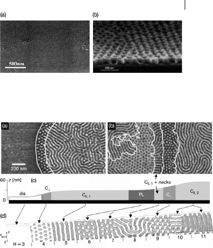
scanning electron microscopy ( SEM ) images shown in Figure 1.8 . Third, the
thickness of the BCP must be carefully controlled. It has been shown that, for
a lamellar PS - b - PMMA BCP, if the initial fi lm thickness t is thicker than the
natural period of the lamellae L
o
and t ≠ ( n + ½) L
o
( n an integer), then islands
or holes of height L
o
will form at the surface of the fi lm and damage the homo-
geneity of the surface morphology. In the case where t < L
o
, the situation becomes
more complicated, as the lamellar chains will arrange perpendicular to the sub-
strate due to the large entropic penalty associated with the chains having to
compress to fi t into the parallel orientation [85] . Other hybrid morphologies
(Figure 1.9 ) have been found as the fi lm thickness changes, due to the competi-
tion of several forces such as strong surface interactions, slow kinetics, and the
thermodynamic driving force to arrange in layers commensurate with the height
L
o
. The physical complexity of block copolymer systems is staggering, and ori-
entational control over these systems has developed into a fi eld of its own [86] .
Many research groups have achieved success in controlling the orientation of
1.2 Block Copolymers as Lithographic Materials 19
Figure 1.8 Field - effect scanning electron microscopy images
obtained from a thin fi lm of PS - b - PMMA after removal of the
PMMA block. (a) Top view of the fi lm; (b) A cross - sectional
view. Reprinted with permission from Ref. [90] ; © 2006,
Wiley - VCH.
Figure 1.9 (a,b) Tapping - mode atomic force
microscopy phase images of thin poly(styrene -
block - butadiene - block - styrene) (PS - b - PB - b - PS)
fi lms on Si substrates after annealing in
chloroform vapor. The surface is covered with
an 10 nm - thick PB layer. Bright regions
correspond to PS microdomains below the
darker top PB layer. Contour lines calculated
from the corresponding height images are
superimposed; (c) Schematic height profi le
of the phase images shown in (a, b);
(d) Simulation of a block copolymer fi lm in
one large simulation box with increasing fi lm
thickness. Reprinted with permission from
Knoll A., Horvat, A., Lyakhova, K.S. et al.
(2002) Phys. Rev. Lett. , 89 , 035501 - 1; © 2006,
American Physical Society.

20 1 Phase-Selective Chemistry in Block Copolymer Systems
the self - assembled structures through special processing strategies; these include
techniques such as thermal annealing [87] , electric fi elds [88 – 90] , mechanical
shear [91 – 93] , exposure to solvent vapor [18, 94, 95] , physical confi nement [96] ,
neutral surfaces [97, 98] , chemically nanopatterned surfaces [99 – 101] , or a com-
bination of any of the above [102] .
1.2.2.1 Creation of Nanoporous Block Copolymer Templates
Once a high degree of long - range ordering has been achieved on a BCP thin
fi lm, a fi nal processing step is necessary to create the nanolithographic tem-
plate. A schematic of BCP lithography is shown in Figure 1.7 b. Upon exposure
to UV, chemical, or reactive ion etching ( RIE ), these systems are designed so
that one of the blocks will be selectively degraded relative to the other block(s).
In fact, the second block should ideally become photochemically crosslinked
and thus highly immobile during the subsequent pattern transfer step in order
to avoid distortion of the photo pattern. Both “ wet ” and “ dry ” chemical proc-
esses can be used during the pattern transfer step. Wet chemical etching
involves the dissolution of the fi rst block in an aggressive acid or base solvent,
whereas “ dry ” chemical processes refer to exposure of the fi lm to high - energy
reactive ions and plasmas such as CF
4
, O
2
, SF
6
, Cl
2
, or argon gas. The etching
process results from the combination of the kinetic energy of the ions (causing
sputtering) and ion - induced chemical reactions that create volatile byproducts.
The etching process affects polymers to different extents, depending on the
chemical composition of the block. Several different types of BCP systems
have been used as nanolithographic templates, such as poly(styrene - block -
butadiene), poly(styrene - block - methyl methacrylate), poly(styrene - block - ferroce-
nyldimethylsilane), poly(styrene - block - lactic acid) and poly( α - methylstyrene -
block - hydroxystyrene). The structures of the most commonly used sacrifi cial
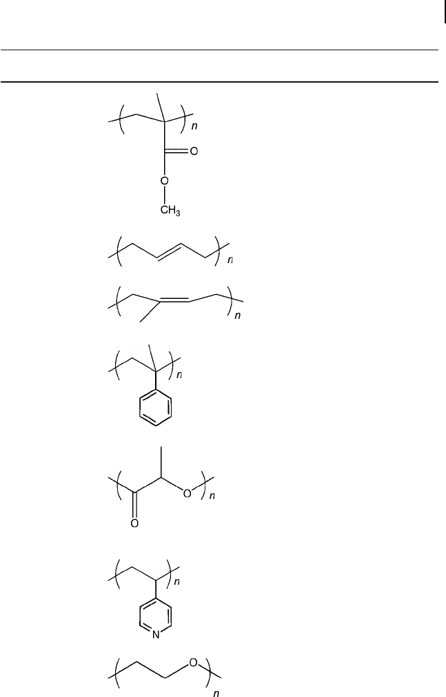
blocks are listed in Table 1.2 .
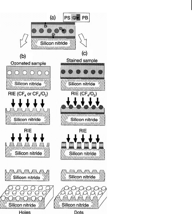
Poly(Styrene - b lock - Butadiene) One of the fi rst applications in this area also pro-
vides a model example of the concept of BCP lithography. Chaikin and coworkers
[80, 111] created a thin fi lm of microphase - separated poly(styrene - block - butadiene)
( PS - b - PB ), as shown in Figure 1.10 a. Figure 1.10 b shows how ozone was used to
eliminate the PB spherical minority phase and open up windows in the PS matrix.
In this instance, the minority PB block acts as a positive - tone resist due to its
vulnerability to ozone chemical attack. The resulting spherical pores in the fi lm
provided less RIE resistance than the continuous PS matrix, thus creating a peri-
odic array of 20 nm holes spaced 40 nm apart on a silicon nitride substrate. In the
opposite strategy, illustrated in Figure 1.10 c, the PB block was stained with
osmium tetroxide vapor, which caused the PB block to exhibit a greater etch resist-
ance than the PS block. In this case, the PB block acts like a negative - tone resist,
resulting in removal of the PS matrix after RIE with CF
4
. Therefore, the negative -
tone system creates a pattern of raised dots on the substrate, instead of holes. This
concept can easily be extended to create nanosized metal dots on any type of sub-
strate for high - density information storage applications [127] , or substrates such
1.2 Block Copolymers as Lithographic Materials 21
Table 1.2 Commonly used sacrifi cial blocks for block copolymer templates.
Name Structure Method of removal Reference(s)
Poly(methyl
methacrylate)
Photolysis [103 – 107]
Etch selectivity [108 – 110]
Poly(butadiene)
Ozonolysis [80, 111, 112]
Poly(isoprene)
Reactive ion etching [113, 114]
Ozonolysis [14, 111, 115]
Poly( α -
methylstyrene)
Heat/Vacuum [116, 117]
Poly(L - lactide)
Aqueous base
dissolution
[118 – 121]
Poly(4 - vinyl
pyridine)
Reactive ion etching [96]
Poly(ethylene
oxide)
Water dissolution [122]
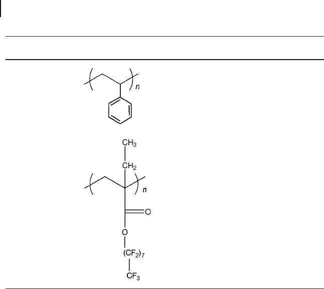
22 1 Phase-Selective Chemistry in Block Copolymer Systems
Name Structure Method of removal Reference(s)
Polystyrene
Reactive ion etching [123, 124]
Poly(perfl uorooctyl
ethyl methacrylate)
Reactive ion etching [125, 126]
Table 1.2 Continued.
as gallium arsenide can be patterned, opening up new avenues for the production
of quantum dot ( QD ) structures [128] .
Poly(Styrene - b lock - Methyl Methacrylate) Poly(styrene - block - methyl methacrylate)
( PS - b - PMMA ) has been the workhorse of the fi eld of BCP lithography for several
reasons. First, it is relatively simple to produce using anionic polymerization
techniques, and is commercially available [129] . Second, PMMA acts as a readily
degradable positive - tone resist on exposure to deep ultraviolet ( DUV ) or e - beam
radiation. In fact, PMMA is already well established in the semiconductor industry
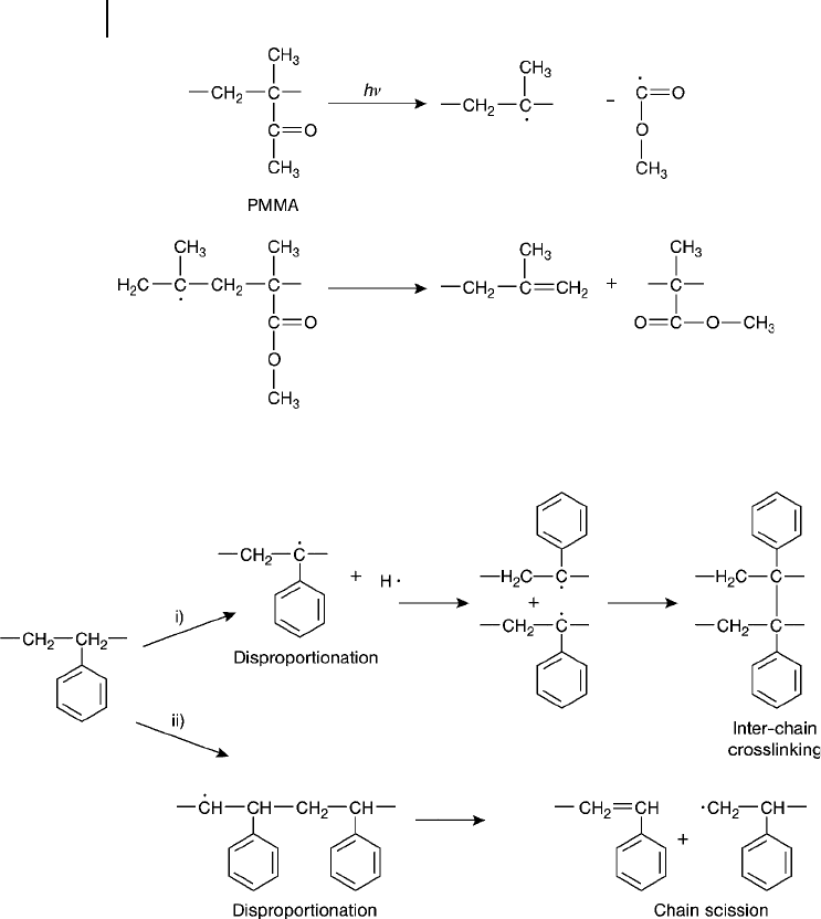
as a positive - tone e - beam resist. The PMMA chain breaks up into oligomers
through a chain scission mechanism (Scheme 1.7 ), and can then be removed from
the matrix through dissolution in acetic acid. Third, in the same DUV exposure
step, the polystyrene matrix acts as a weak negative - tone resist, becoming photo-
chemically crosslinked through oxidative coupling, as shown in Scheme 1.8 [130] .
Immobilizing the matrix phase through crosslinking strategies is very important
in the creation of nanoporous materials. The huge increase in surface area that
results from the removal of the minority domain creates a concomitant increase
in surface free energy. A driving force for the minimization of this free energy
creates a strong tendency for the nanopores to collapse, which would result in
distorted etched patterns. A high glass transition temperature ( T
g
) relative to the
processing temperature represents another means of stabilizing the nanoporous
1.2 Block Copolymers as Lithographic Materials 23
template; however, there must be a clear pathway in the fi lm for the removal of
degraded minority component (e.g., vertical cylinders). Otherwise, the low - molec-
ular - weight products permeate through the matrix, leading to a decrease in T
g
and
collapse of the pores.
Stoykovich and colleagues in the Nealey group have substantially improved the
directed self - assembly of lamellar microdomains of PS - b - PMMA. Traditional
lithographic techniques were used to create a chemically nanopatterned surface
that preferentially wets the PMMA domain. By using this preferential attraction,
Figure 1.10 (a) Schematic cross - sectional
view of a nanolithographic template
consisting of a uniform monolayer of PB
spherical microdomains on silicon nitride.
PB wets the air and substrate interfaces;
(b) Schematic of the processing fl ow when an
ozonated copolymer fi lm is used, which
produces holes in silicon nitride;
(c) Schematic of the processing fl ow when
an osmium - stained copolymer fi lm is used,
which produces dots in silicon nitride.
Reprinted with permission from Ref. [80] ;
© 1997, American Association for the
Advancement of Science.
24 1 Phase-Selective Chemistry in Block Copolymer Systems
Scheme 1.7 Chain scission mechanism of PMMA.
Scheme 1.8 Ultraviolet irradiation byproducts of polystyrene.
Stoykovich et al . were able to steer the vertically oriented lamellar morphologies
through various bend angles, from 45 ° to 135 ° (Figure 1.11 ). The high curvature
of these patterns induces a great deal of stress in the in the polymeric material,
and leads to the formation of defects in the structure. It was found that, by blend-
ing small amounts of PMMA homopolymer, the homopolymer selectively swelled
the PMMA block in the areas of high curvature (Figure 1.11 b); this alleviated the
stress in the material and in turn reduced the pattern defects [131] .
Several successful applications of PS - b - PMMA as a nanolithographic template
have already been achieved, with C. T. Black and coworkers at IBM being among