Curry G.L., Feldman R.M. Manufacturing Systems Modeling and Analysis
Подождите немного. Документ загружается.


Problems 233
q = 1/3,
1 −q = 2/3 .
Workstation 3 (batch move):
E[ T
s
(I)] = 1/5,
C
2
[T
s
(I)] = 1/2 .
7.10. Consider a factory with a batch server. Let the network structure be the same
as that of Fig. 7.4, except that the branching probabilities are different. The data
for the workstations and the branching probabilities are given below. Develop the
workstation and system performance measures of throughput, cycle time and work-
in-process. The external arrival process is assumed to be Poisson. Note: use (7.25)
in the C
2
a
(I) term.
Workstation Inflow Machines Batches E[T
s
] C
2
[T
s
]
110211/252
2 0 1 1 1/35 2
3 0 1 4 1/10 2
From/To 1 2 3
101/32/3
2 1/3 0 1/3
3 4/10 6/10 0
7.11. Consider a network of four workstations with the data given in the following
tables. Draw the network diagram and develop the workstation and system perfor-
mance measures of throughput, cycle time and work-in-process. The external arrival
process is assumed to be Poisson.
(a) Use Property 7.7 in the C
2
a
(I) computations.
(b) Use Eq. (7.25)intheC
2
a
(I) computations.
Workstation Inflow Machines Batch Size E[T
s
] C
2
[T
s
]
1 2.5 1 1 0.10 2.00
2 1 2 1 0.26 1.50
3 0 1 1 0.13 0.75
4 0 1 4 0.64 3.00
From/To 1 2 3 4
1 0 2/4 1/4 1/4
2 1/301/31/3
3 4/8 1/8 0 1/8
4002/30
7.12. A manufacturer produces two products in a three-workstation facility. The
products are similar and both use an identical heat-treatment process. Thus, these
products can be indiscriminately mixed for this oven process, that can process six

234 7 Models of Various Forms of Batching
items simultaneously. Both external arrival processes are Poisson distributed. The
factory capacity consists of 5 identical machines in Workstation 1, 4 identical ma-
chines in Workstation 2, and one oven for the heat-treatment process in Worksta-
tion 3 (with a batch capacity of 6 jobs). Using the product branching probabilities
and processing time data listed below, compute the factory cycle time, work-in-
process and throughput. All times are in hours. Note: use Eq. (7.25)intheC
2
a
(I)
computations.
Product 1
Workstation Inflow Batch Size E[T
s
] C
2
[T
s
]
1 2 1 0.20 1.00
2 0 1 0.30 1.50
3 0 6 0.40 1.75
Product 1
From/To 1 2 3
101/21/2
2 1/403/4
31/31/30
Product 2
Workstation Inflow Batch Size E[T
s
] C
2
[T
s
]
1 3 1 0.30 2.00
2 0 1 0.35 1.80
3 0 6 0.40 1.75
Product 2
From/To 1 2 3
102/31/3
2 1/302/3
33/500
7.13. Re-derive the batch service time process characteristics C
2
[T
s
(B)] (Eq. 7.18)
using Property 1.9 for the sum of random variables.
7.14. Team Project Problem. The Southwestern Specialties Company has a line of
four products that they produce in their factory located in Houston, Texas, working
24 hours per day. The company is soliciting bids from consulting firms for the anal-
ysis of their current and future factory performances. The company currently has
contracts with several national retail companies, such as Wal-Mart, Kmart, and Tar-
get, to produce specific quantities of each of their four products. The initial project
phase is to develop a model of their current factory and develop cycle time estimates
for each product. The second phase of the project will be to predict the impact of a
new marketing strategy based on E-Commerce using the World-Wide-Web. Several
consulting companies have been selected to perform the first phase of the project
(current factory performance modeling) and the best among those will be selected

Problems 235
for the future phase. Only after successfully demonstrating your consulting firms
capabilities, will the company authorize the release to the consulting firm the nature
of the second phase of the modeling and analysis project.
First Phase Information
The Southwestern Specialties Company’s Houston factory consists of three
workstations (called Workstations 1, 2 and 3). Workstation 3 is an oven heat-
treatment facility. The four products take different routes through the three work-
stations and have different numbers of processing steps. There currently are three
machines in Workstation 1 and one machine each in Workstations 2 and 3. The
machine (oven) in Workstation 3 has the capacity to process up to 4 units simulta-
neously, but it is currently operated with a fixed batch size of 3 units. Engineering
has spent considerable design and analysis time over the years to develop a process-
ing procedure that allows all four of the products to be processed in the oven with
the same time and temperature settings. Therefore, the factory operations personnel
can form an oven batch from any combination of the four product types.
Orders are released to the factory according to a Poisson process at a mean rate
of 7.68 orders per day. The current distribution of order releases by product type is
(20%, 30%, 25%, 25%) for Products, 1, 2, 3 and 4, respectively.
Engineering has developed standard times for each of the processing steps for
each product and these “mean” times are listed below. Their analysis has revealed
the surprising fact that the distribution of processing times for each and every pro-
cess is very accurately approximated by an Erlang Type-2 distribution. The work-
stations’ sequence for each product is:
Products 1 2 3 4 5
1 3121
2 12321
3 21231
4312
The mean processing time by product and processing step, in hours, are:
Products 1 2 3 4 5
1861.76
2 51.681.55
3 1.9 4 2.2 8 4
4832.2
The average cycle time for all products is approximately 80 hours. The consult-
ing firms will be selected to continue into the second modeling and analysis phase
based on their answer to the question: What is the mean cycle time by product? Of
course, all relevant data concerning your firms answer to this question must be pro-
vided.
Second Phase Information
Your consulting firm has been selected to analyze the new company strategy for
the Southwestern Specialties Company. The company has decided to no longer use
236 7 Models of Various Forms of Batching
Product 1
1
2
38
0.10
0.15
4
5
1 2
3
0.05
losses
0.07
Fig. 7.5a Process flow diagram for Product 1 of Problem 7.15
1 2
34
1
2
3
5
losses
0.04
0.090.08
0.05
2
Product 2
Fig. 7.5b Process flow diagram for Product 2 of Problem 7.15
fixed contracts. They have decided that they would do better by selling the four
products over the internet. The research staff has determined that the sales rates are
functions of the product cycle times and they estimate these functions as:
Product 1: r(1)=0.1088 −0.0006 ×CT(1),
Product 2: r(2)=0.1632 −0.0007 ×CT(2),
Product 3: r(3)=0.1360 −0.0006 ×CT(3),
Product 4: r(4)=0.1360 −0.0009 ×CT(4).
The company will allow two new machines to be purchased of any type (exclud-
ing ovens). The company wants answers to the following questions:
(a) What should be the company capacity structure?
(b) What is the projected company sales rates and cycle times for the four products?
(c) Are the s ales consistent and stable? If not what can be done to make them stable?
(d) Is the company in a good or bad situation?
7.15. Team Project Problem. Quality Products Inc., a company that manufactures
high-quality heat-pumps for the housing industry, has a local manufacturing facil-
ity. This plant only produces heat-pumps and until recently there was only one ba-
sic production process for these items. With the new environmental concerns and
government regulations, they have designed and recently brought into production a
second product line of heat-pumps. The production processes for the old and new
product lines are similar, using the same equipment, but they have slightly different
processing sequences and processing times. The product processing sequences are
illustrated in Figs. 7.5a and 7.5b. Product 1 is the old heat-pump process and Prod-
uct 2 is the production sequence for the new line of heat-pumps. This first quarter
of 2002 the daily releases of products to be manufactured is 8 units on the product
1 and 2 units of Product 2. The average cycle time for the facility is in the neighbor-
hood of 6.2 days.

Problems 237
Quality Products Inc. would like to have a consulting team perform a systems
analysis for each quarter of the year. They expect that the t otal of units manufactured
to remain at a demand level of 10 per day but the product mix will change each
quarter. Their quarterly demand forecasts for daily demands by product type are:
First Quarter Second Quarter Third Quarter Fourth Quarter
Product 1 8 6 4 2
Product 2 2 4 6 8
The company is concerned about their machining capacities as demands change
over time. They would also like to know what the impacts will be on their cycle
times and they want to estimate the cycle times for the individual products as well
as the facility average. If new machines are needed, they want to get these ordered
and installed so that they will not suffer a short-fall in production output versus
demand.
The top-planning engineer for Quality Products Inc. has developed the data for
the old and new product processing steps. The mean processing times (in days) are:
Means Step 1 Step 2 Step 3 Step 4 Step 5 Step 6 Step 7 Step 8
Product 1 0.008 0.120 0.070 0.070 0.075 0.100 0.070 0.180
Product 2 0.002 0.100 0.090 0.070 0.080 0.080 0.070 0.100
SCV’s Step 1 Step 2 Step 3 Step 4 Step 5 Step 6 Step 7 Step 8
Product 1 1.5 1.2 1.3 1.0 1.6 0.9 1.3 0.5
Product 2 1.0 1.0 1.0 1.3 1.0 1.0 1.3 1.0
There are currently three machines in Workstation 2 and two machines at Work-
station 5. The other workstations seem to be operating okay with a single processing
machine. Workstation 3 is a heat-treatment process and the current capacity of the
machine is two jobs at a time.
The product demand data is currently 8 units of Product 1 per day with a SCV
of 1.5. Product 2 has a mean demand rate of 2 units per day with an SCV of 0.75.
As demand shifts from being predominantly Product 1 to mostly Product 2, the
company does not anticipate a change in the SCV’s for the individual products.
All of the machines in the factory have a 95% availability factor. The mean repair
times are, respectively, 0.2, 0.3, 0.4, 0.35, 0.5, days. All repair times are exponen-
tially distributed.
7.16. Team Project Problem. The MicroTex Corporation makes special purpose
microprocessors that are used in a variety of machines. The company produces two
products as variants from the same processing procedure. The products are distin-
guished after one layer or single sequence through the processing steps. After the
first layer has been completed, the wafers go through a test operation; wafers are
238 7 Models of Various Forms of Batching
characterized as worthless (waste), bad and in need of rework, good wafers but low
cycle speeds, and excellent with high cycle speeds. Product 1 is made from the low
cycle speed processors that are immediately packaged and shipped. The high-speed
units are processed further by a second sequence through the basic operational steps
(using the same machines as previously) and then a final test is performed. Units
again are characterized as waste, rework and completed units (no low speed units
can come out of the second test). The completed units are then packaged and shipped
as the company’s high-grade product.
Microprocessor chips are produced by a process that starts with pure silicon
wafers that are fragile, flat, thin circular objects that look similar to glass. Patterns
are placed on the wafers by covering them with a photo-resist material and then ex-
posing the images onto the resist by shining light through a template or mast of the
desired image. The images are hardened by baking the wafer in an oven. A pattern
of holes is then etched into the mask layer by removing the exposed material. This
allows the dopants to be diffused into selected areas of the wafer. Specific ion atoms
(dopants) are implanted on the exposed surface (boron, phosphorous, and arsenic)
by diffusion processes. These processes are repeated hundreds of times to produce
a state of the art microprocessor. Then a wafer probe is used to functionally test the
individual processors on the wafer and characterize their performance potential. The
completed wafers are diced into single chips with a diamond saw and then attached
via glue to a package. The package provides the contact leads to the chip. Wire
bonding, generally with gold leads, is used to connect the package leads to the wire
connections within the chip. Then the package containing the chip is encapsulated
with a plastic coating for mechanical and environmental protection.
The MicroTex wafer fab is a state-of-the-art pilot facility with the latest cluster
tool technology. These fabrication processes are performed in three basic steps. The
first set of processing steps is performed in Workstation 1 with a pair of identical sin-
gle wafer processing equipment (machines). At the second workstation, the remain-
ing set of operations is performed in a batch mode using a single large capacity (up
to eight lots simultaneously) processor (similar to an oven operation). A third work-
station contains a single testing machine used to determine the wafer performance
characteristics. Workstation 4 consists of the packaging operations also performed
using a single piece of equipment. All of the completed products received the same
general processing using the same equipment, although the processing times vary
for the second production pass. The wafer units that have graded out as high quality
and speed are processed further.
To prepare for the second layer, the second time through the processing steps, a
separate distinct set of processing must be performed. This preparation processing
step is distinct from previous processing and, therefore, these operations are per-
formed on a separate machine in Workstation 5. When completed, these units are
sent back through the first three workstations for another sequence of processes. The
second sequence of processing has distinct times from those of the first sequence,
except for the batch operations of Workstation 2. This is fortunate, allowing batch-
ing at Workstation 2 to be indiscriminate of the type of wafers being processed.
That is, batches can consist of either or both types of wafers. If the high quality
Problems 239
product wafers grade out acceptably they are also then packaged at Workstation 4
and shipped.
Phase I
MicroTex management would like your consulting team to develop a model of
their facility and help them answer questions concerning potential areas of improve-
ment. The first phase of the project is to utilize their best guess data, compiled by
their lead engineers, and develop a preliminary model of their company. If they
find this result acceptable, they will allow your team access to the actual company
proprietary data from which accurate and meaningful data can be developed. This
refined model will then be used to develop strategies for future company improve-
ment and new product development. These types of facility are extremely expensive
to build, frequently costing from one to two billion dollars for a full scale facility.
Thus, continuous operation of the facilities is maintained at all times; 24 hours a
day, s even days a week.
The work release rate for the pilot facility is one job (lot of 24 wafers) per hour.
All times are given in lot units. The mean times for the first three processing steps
are estimated to be 1.15, 2 and 0.25 hours, respectively. The test operation on aver-
age finds that 10% of the processed wafers are scrapped and 15% can be reworked
and are thus reprocessed at Workstation 2. Of the acceptable units, only 1/3 grade
out as high quality and speed and go through further processing. The packaging
operation for the low or first level product takes 45 minutes while the high quality
product takes 54 minutes. For the high quality product, the unique first additional
step takes 2 hours and 15 minutes. The company policy is that when (on the first
trip through only) a l ot is scrapped, it is replaced with a new lot start. The second
trip through workstation one takes 75 minutes and in Workstation 3 the second trip
requires an additional 3 minutes over the first processing time. The batch size used
in Workstation 2 is a fixed quantity of four jobs (four lots of wafers). This is a car-
ryover from a previous production line where the machine capacity was limited to
four lots. For the pilot factory, the number of machines in Workstation 1 is two, the
number of ovens in Workstation 2 is one, and the number of machines in Worksta-
tion 3 is one. For this pilot system analysis, we can assume that the order release
process (external arrival process) and all service processes have squared coefficients
of variation with values of 1.
MicroTex wants a short written report of your consulting team’s preliminary
model to determine if your consulting team will be continued into the actual fac-
tory analysis phase.
Phase II
The MicroTex Corporation accepts your design team as the company’s consulting
team for the wafer fabrication pilot facility study. During your preliminary analysis
period, the company has had a team of industrial engineering coop students collect-
ing time study data for all the machines used in the facility. The coop group finished
the analysis on four of the five machine types and furnished the following table:

240 7 Models of Various Forms of Batching
Processing Step E[S] C
2
s
11.15hr3
2(oven) 2hr 2
3 ( test) 0.25 hr 1
4 (package) 0.75 hr 4
5 (special) 2.25 hr 3.05
6 (1) 1.25 hr 3
7(oven) 2hr 2
8 ( test) 0.30 hr 1
9 (packaging) 0.90 hr 4
The current pilot facility has a cycle time around 65-70 hours. Management has
a quality improvement program in place and they predict that scrap losses can be
reduced to 5%, rework can be reduced to 10%. In addition, engineering believes
that the processing times variations can be reduced across the board by 50%. Can
the management goal of a cycle time of less than 35 hours be reached?
Engineering is always working to improve the high speed wafer yield percentage.
These units are worth considerably more and have an unlimited market. Engineering
feels that this yield percentage can be drastically improved, but maintaining the
cycle time goal of 35 hours will be impossible. Management has, therefore, agreed
to allow one more machine (of any type) to be placed in the pilot facility if necessary.
What is the maximum high speed wafer yield percentage that can be accommodated
within the 35 hour cycle time guideline?
The real goal of the pilot facility is to determine what facility configuration is
necessary for a full scale facility with a release rate of 10 lots per hour. We can
assume that all of the learning with respect to yields, variation reductions, etc., carry
over to the new facility. Assuming that the best yield results for the pilot facility can
be maintained in the new plant, what is the machine configuration and estimated
cycle time for this facility?
References
1. Albin, S.L, and Kai, S. (1986). Approximation for the Departure Process of a Queue in a
Network. Naval Research Logistics Quarterly, 33:129–143.
2. Cooper, R.B. (1990). Introduction to Queueing Theory, Third Edition. The MacMillan Com-
pany, New York.
3. Curry, G.L., and Deuermeyer B.L. (2002). Renewal approximations of the departure processes
of batch systems. IIE Transactions, 34:95–104.
4. Curry, G.L., and Feldman, R.M. (1985). An M/M/1 Queue with a General Bulk Service Rule.
Naval Research Logistics Quarterly, 32:595–603.
5. Hopp, W.J., and Spearman, M.L. (1996). Factory Physics: Foundations of Manufacturing Man-
agement. Irwin, Chicago.
6. Buzacott, J.A., and Shanthikumar, G.J. (1993). Stochastic Models of Manufacturing Systems.
Prentice-Hall, Englewood Cliffs, New Jersey.

Chapter 8
WIP Limiting Control Strategies
Many companies find themselves with too much work-in-process. The disadvan-
tages of high levels of WIP are numerous, and many of the disadvantages cannot
be directly measured economically. Two major disadvantages of high WIP levels
that are difficult to economically evaluate are not being able to r espond to demand
changes quickly and the potential to build a considerable quantity of poor qual-
ity stock before realizing that there is a quality problem. To help control inventory
within production and manufacturing facilities, WIPlimiting production procedures
are frequently used.
The just-in-time production approach attempts to control product releases based
on factory conditions. The production release approach studied to this point is based
on a schedule or “push” approach. The “pull” production strategy, generally associ-
ated with the Toyota production controls, was originally based on a card or kanban
system. (The term kanban, borrowed from the Japanese language, originally referred
to the use of cards to control the movement of parts; however, today many things
other than cards might be used including simply an empty cart or even golf balls.)
The general concept is to release work only when something has left the system
(area or range of oversight control). This approach is thus some form of a WIP lim-
iting process. One of the simplest approaches is to limit the total WIP and not be
concerned with allocation restrictions within the facility itself. This approach, pop-
ularized under the term CONWIP from CONstant WIP (see Hopp and Spearman
[8]), puts a new job into the system whenever a job leaves the system after the sys-
tem has reached its CONWIP level. Once the system is loaded to the desired limit,
this approach maintains a constant WIP in the system. More detailed controls can
be accomplished by restricting the WIP available in regions of the factory and even
down to the workstation level. When the CONWIP approach is implemented for
each workstation, it becomes conceptually equivalent to the kanban approach.
Two different approaches for facility control are studied in this textbook: CON-
WIP and kanban control policies. This chapter considers a total WIP limit ap-
proach via the mathematical methodology of closed queueing networks. In Chap. 9,
WIP limits at individual workstations or kanban control are studied. These two ap-
proaches lead to different analytical models for predicting the system performance
G.L. Curry, R.M. Feldman, Manufacturing Systems Modeling and Analysis, 2nd ed., 241
DOI 10.1007/978-3-642-16618-1 8,
c
Springer-Verlag Berlin Heidelberg 2011
242 8 WIP Limiting Control Strategies
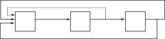
Fig. 8.1 Closed queueing
network example
12
3
9/10
1/10
1/10
9/10
measures. The CONWIP method is the simpler mathematically as well as the sim-
pler to implement and can be studied by the well developed approximation area
called mean-value analysis for closed queueing networks. Mean value analysis is a
computationally simple approach that was developed for exponential service time
models. An approximation for general service distributions called extended mean
value analysis is also discussed.
This chapter is concluded with a case study of the impacts of CONWIP control
along with several job sequencing algorithms for selecting the next job from the
queue for processing. This study is presented to familiarize the reader with the po-
tential impact that scheduling rules, other than just push or pull strategies, can have
on factory performance.
8.1 Closed Queueing Networks for Single Products
In Chap. 5, queueing networks were used to represent a factory. These were open
queueing networks because jobs arrived from a source external to the network and
jobs departed from the network. We will now change this approach and use closed
queueing networks to model the factory.
Definition 8.1. A closed queueing network is a network of queues in which no ar-
rivals are possible from outside the network and no jobs within the network can
leave.
The network displayed in Fig. 8.1 is an example of a closed queueing network.
A closed queueing network is a representation of a constant WIP controlled system
where the total WIP is set at a specified limit, say w
max
. When a job completes
service, it is counted and a new job is entered into the system immediately. This
is mathematically equivalent to branching the completed job back to the starting
workstation. For this representation of a constant WIP system, there are no external
flows into the system and really no exiting flows from the system. Job completions
are counted by recognizing that the rate of “good” jobs leaving the last workstation
is equivalent to a job completion. The term “good” implies that a proportion of
the jobs leaving the last workstation could be defectives that are not counted as
completed jobs and these may be branched back for rework or, if scrapped, then a
totally new job is started in the defective job’s place.
Example 8.1. Consider a three-workstation factory where all jobs leaving Worksta-
tion 1 are sent to Workstation 2. From Workstation 2, 10% must be reworked and are