Cooper L.N., Feldman D. (Eds.) BCS: 50 Years
Подождите немного. Документ загружается.

September 8, 2010 10:53 World Scientific Review Volume - 9.75in x 6.5in ch9
SQUIDs: Then and Now 151
Brian Pippard wandered into our lab to see how things were going, and Paul
and I proudly showed him one of our new gadgets. Brian contemplated it
thoughtfully for a while, and then — with a smile — said, “It looks as though
a slug crawled through the window overnight and expired on your desk!”
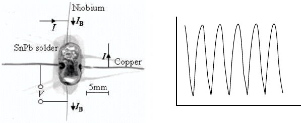
I tried hard to make a SQUID by freezing a solder blob on a piece of
niobium wire doubled back on itself so that there were two junctions. I ap-
plied a magnetic field to the loop of wire sticking out of the solder blob. This
never worked, in retrospect because the inductance of the loop was too high.
One day, I decided instead to pass a current along the wire, and immediately
saw oscillations in the critical current when I changed the current. It did
not take me very long to discover that the loop was irrelevant — I needed
to pass the wire through the solder only once, and apply a current to the
wire [Fig. 3(a)]. How did it work? Apparently, there were typically just two
or three dominant junctions between the wire and the solder. The current
in the wire generated a magnetic field in the penetration depths of the wire
and solder, so that the area of the “SQUID” was given by the sum of the
penetration depths times the separation of the junctions. The periodicity
in current ranged randomly from about 0.2 to 1 mA. However unlikely, the
majority of these devices showed interference between two or three junctions,
and they generally survived at least scores of thermal cyclings. It is inter-
esting to note that, as I increased the current through the niobium wire,
I could generally observe thousands of oscillations in critical current with
no evident diminution in amplitude. This lack of a discernible Fraunhofer
pattern suggested that the junctions were essentially points.
The name for this new device had already been unwittingly provided by
Brian Pippard and we simply had to work out what it stood for. And so the
“Superconducting Low-inductance Undulatory Galvanometer” (SLUG) was
born.
Brian’s original concept was a digital voltmeter, but I soon realized that
one could readily measure changes in flux that were much less than one flux
quantum. I applied a static current and a sinusoidal current through the
SLUG [leads “I” in Fig. 3(a)] so that voltage pulses appeared across the
voltage leads [leads “V ” in Fig. 3(a)]. The area under these pulses depended
on the critical current of the SLUG, enabling me to determine the critical
current, and hence the current in the niobium wire [leads “I
B
” in Fig. 3(a)]
to about ±1 µA, using simple electronics. Once I had this worked out, I
immediately put the SLUG together as a voltmeter. A postdoctoral fellow
in the Mond, Steve Lipson, was interested in measuring the resistance of a
single crystal of copper (to be used for measurements of magnetoresistance)
September 8, 2010 10:53 World Scientific Review Volume - 9.75in x 6.5in ch9
152 J. Clarke
Current I
B
in niobium wire
Voltage
(a) (b)
Fig. 3. The SLUG. (a) Photograph showing attachment of current (I), voltage (V)
and flux bias (I
B
) leads. (b) Voltage V versus I
B
.
that he estimated to be about 10
−8
Ω. We made a voltmeter by connecting
the Cu block in series with a manganin wire, with a measured resistance of
about 10
−5
Ω, and the niobium wire through the SLUG. The idea was to
make a potentiometer, adjusting the currents in the two resistors to produce
zero current in the SLUG. After Steve and I cooled down our potentiometer,
I was chastened to observe that the output from the SLUG was horribly
noisy. Further inspection showed that the “noise” was in fact due to cur-
rents induced in the loop by 50-Hz magnetic fields. For the next run, Steve
soldered up some lead foil to make a box that enclosed the circuit, and our
pickup problem was solved. This was an invaluable lesson for me: if you
have a sensitive magnetometer or voltmeter, you have to protect it from the
real world, which is a very noisy place.
I used the SLUG as a voltmeter for the rest of my graduate career, mostly
to investigate SNS Josephson junctions.
17
With a typical circuit resistance
of 10
−8
Ω, I could measure a voltage of about 10
−14
V in a second. Other
members of the Mond subsequently used the SLUG, notably Eric Rumbo
18
for measuring thermoelectric voltages and Pippard, Shepherd and Tindall
14
for measuring the resistance of the SN interference — my original thesis
topic.
I moved to the Physics Department at the University of California, Berke-
ley in January 1968 as a postdoctoral scholar, and used SLUGs in various
measurements. I devised an experiment to test the accuracy of the Josephson
voltage-frequency relation in junctions made from different superconductors.
I irradiated two SNS junctions with the same radiofrequency magnetic field,
and measured the voltage difference between steps of a given order induced
on the two I-V characteristics. I found that the voltages were the same to
September 8, 2010 10:53 World Scientific Review Volume - 9.75in x 6.5in ch9
SQUIDs: Then and Now 153
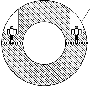
000-120 SCREW
AND NUT
Fig. 4. Point contact dc SQUID. (Reproduced with permission from Ref. 25.)
an accuracy better than 1 part in 10
8
, corresponding to a voltage difference
of less than 2 × 10
−17
V, regardless of the nature of the superconductor.
19
This result helped to establish the Josephson junction as a means of main-
taining the standard volt in terms of a frequency.
20
Much later, Shen Tsai
and co-workers
21
repeated the experiment to the remarkable accuracy of two
parts in 10
16
.
Subsequently, I used a SLUG voltmeter to measure the pair-quasiparticle
potential difference in nonequilibrium superconductors.
22
Single electrons
tunneling from a normal electrode into a superconducting film generate
an imbalance between the electron-like and hole-like quasiparticles. This
“charge imbalance” is detected by a normal electrode in tunneling con-
tact with the reverse side of the superconductor: a voltage is induced on
the normal electrode relative to the chemical potential of the Cooper pairs
measured some distance away from the nonequilibrium region of the super-
conductor. Shortly after I had completed this experiment, in early 1972 I
returned to the Mond Laboratory on sabbatical leave. Mike Tinkham was
also there on leave, writing his celebrated book on superconductivity, and he
worked out the theory of charge imbalance.
23
Subsequently, charge imbal-
ance was investigated in a variety of other nonequilibrium superconducting
configurations.
24
During the time I was working on the SLUG, Zimmerman and Silver
25
were busily developing the “point contact” dc SQUID, shown in Fig. 4. The
body was machined from niobium, and the two halves were clamped together
with a thin insulator separating them. The junctions were formed by two
sharpened niobium screws that could be adjusted from outside the cryo-
stat to provide optimal current-voltage characteristics. This simple means
September 8, 2010 10:53 World Scientific Review Volume - 9.75in x 6.5in ch9
154 J. Clarke
Am-
plifier
Lock-in
detector
Inte-
grator
Oscillator
I
b
V
f
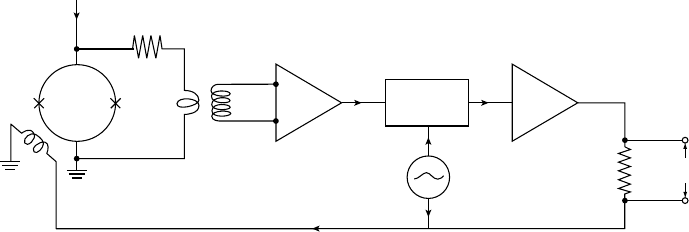
Fig. 5. dc SQUID in flux-locked loop.
of making a Josephson junction or SQUID was emulated in many laborato-
ries. Single-junction versions were used by undergraduates
26
to demonstrate
constant-current steps induced by microwaves on the current-voltage charac-
teristics at voltages nhf/2e (n is an integer, f is the microwave frequency),
and thus verify the Josephson ac relation to an accuracy of 1% or better.
The observation of oscillations in voltage as the flux was varied was a
beautiful piece of physics, but for practical applications, one needs a linear
response. I built and operated a version of the flux-locked loop,
27
but a better
one — that is still used today — was developed by Robert Forgacs and Alan
Warnick
28
at the Ford Laboratory. Feedback serves several purposes: it
makes the response linear in the applied flux, it allows one to track changes
in flux corresponding to many flux quanta, and it enables one to detect
flux changes of a tiny fraction of a flux quantum. As illustrated in Fig. 5,
a sinusoidal magnetic flux with a peak-to-peak amplitude of Φ
0
/2 and a
frequency f
m
of 100 kHz is applied to the SQUID. When the static flux in
the SQUID is nΦ
0
, the resulting oscillating voltage across it is a “rectified”
sine wave, with no component at f
m
. When this signal is coupled to a
lock-in detector referenced to the same oscillator, the output is zero. When,
on the other hand, the static flux in the SQUID is increased from nΦ
0
to
(n + 1/4)Ω
0
, there is a steady increase in the amplitude of the component
at f
m
, and an increasing (say) voltage out of the lock-in. If instead, we
decrease the static flux from nΩ
0
, the voltage out of the lock-in is negative.
The output from the lock-in detector is smoothed, and fed back via a resistor
into a coil inductively coupled to the SQUID. The action of the flux-locked
loop is to maintain the sum of the applied and fed-back fluxes in the SQUID
at a constant value. A flux δΦ
a
applied to the SQUID is canceled by an
opposing flux −δΦ
a
from the flux-locked loop. The output voltage V
f
across
the feedback resistor is proportional to δΦ
a
. In the early days, a typical

September 8, 2010 10:53 World Scientific Review Volume - 9.75in x 6.5in ch9
SQUIDs: Then and Now 155
flux noise was of the order of 10
−3
Φ
0
Hz
−1/2
(“per root Hz”) — meaning
an integration time of 0.25 s — at frequencies where the noise is white. At
lower frequencies, f, the noise spectral density scales approximately as 1/f.
This ubiquitous “1/f noise” or “flicker noise” is still actively investigated
today. Virtually all SQUIDs — except those used at high frequencies — are
operated in a flux-locked loop. There are several other schemes, at least one
of which does not involve flux modulation.
29
3. Early rf SQUIDs
Shortly afterwards, in 1967, the rf SQUID
30
appeared. This device involved
only a single Josephson junction, and the first version was based on the
machined niobium dc SQUID (Fig. 4), with one junction shorted. The rf
SQUID was coupled to the inductor of a resonant circuit [Fig. 6(a)]. When
the tank circuit was driven with a radio-frequency current at the resonant
frequency, typically 30 MHz, the behavior shown in Fig. 6(b) was observed.
31
Here, the voltage across the tank circuit has been amplified, rectified with
a diode and smoothed, so that one observes the amplitude of the rf signals.
When the flux in the SQUID is nΦ
0
, one sees a series of “steps and risers”
as the rf drive is increased. At (n + 1/2)Φ
0
, the steps split into a half-step
above and below the steps. Thus, when the SQUID is biased at the midpoint
of one of the steps the voltage is periodic in the applied flux, as shown in
Fig. 6(c); needless to say, the period is Φ
0
. From this point of view, the
rf SQUID behaves operationally as a dc SQUID. Particularly in those early
days, when making a Josephson junction was a challenge, the fact that the
(b)
(c)
(a)
(a)
Fig. 6. The rf SQUID. (a) Schematic of rf SQUID and its readout circuit. (b) Steps
and risers: Amplitude of rf signal across the tank circuit versus rf drive current for
two values of applied flux. (c) Amplitude of rf signal across the tank circuit versus
applied flux for four values of drive current. [(b) and (c) reproduced with permission
from Ref. 31.]
September 8, 2010 10:53 World Scientific Review Volume - 9.75in x 6.5in ch9
156 J. Clarke
rf SQUID required only a single junction gave it an edge over the dc SQUID.
The rf SQUID is actually misnamed, however, as no interference takes place!
4. Tunnel Junctions Revisited
During the early 1970s, there was a general shift towards using the rf SQUID.
SQUIDs made of thin films deposited on cylindrical substrates,
32,33
with a
narrow microbridge as the single junction, achieved a white flux noise of
about 2 × 10
−4
Φ
0
Hz
−1/2
. The strong dependence of the critical current
of the microbridge on temperature, however, limited the operating temper-
ature range. Such devices, as well as machined niobium devices, became
commercially available.
While on sabbatical leave in the Mond in 1972, I wrote a review article
on SQUIDs.
34
At the time, there was no theory for flux noise in either the
dc or rf SQUID, but I made a simple estimate for the dc SQUID assuming
that the noise arose from Nyquist noise in the junction resistances. This led
me to conclude that the flux noise should be a few µΦ
0
Hz
−1/2
, far lower
than anything that had been achieved. I concluded that the flux noise was
dominated by voltage noise in the preamplifier connected to the SQUID,
and that an appropriate matching network might significantly improve the
performance.
After I returned to Berkeley, a new postdoctoral scholar, Wolf Goubau,
and a new graduate student, Mark Ketchen, and I set to work. We bor-
rowed three ideas from the rf SQUID: a cylindrical geometry (which gives
a large area for a low inductance), a tank circuit readout and thin films.
I had wanted to move away from microbridge junctions because of their
narrow temperature range of operation. Fortunately, Paul Hansma, at the
University of California, Santa Barbara, had achieved good reproducibility
and longevity with Nb-NbOx-Pb tunnel junctions.
35
We decided to copy this
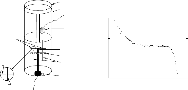
technique, and acquired a sputtering system to deposit niobium. Figure 7(a)
shows the geometry of our SQUID, grown on a 3-mm-diameter quartz tube.
We used shadow masks to pattern the various films, which had a minimum
linewidth of 75 µm. We first deposited the PbIn cylinder, followed by the
gold film that formed the resistive shunt for each junction (to eliminate hys-
teresis on the current-voltage characteristic). We next sputtered the Nb
film, which we oxidized in air in a closed oven (12 min at 130
◦
C was the
recipe). Immediately afterwards, we deposited the PbIn “T” that completed
the junctions. We scribed a slit in the PbIn cylinder with a razor blade.
Subsequently, we submerged the SQUID in a solution of Duco cement
September 8, 2010 10:53 World Scientific Review Volume - 9.75in x 6.5in ch9
SQUIDs: Then and Now 157
QUARTZ TUBE
LEAD BAND
LEAD T
GOLD SHUNT
INDIUM
CONTACT
FREQUENCY (Hz)
(b)(a)
10
−4
10
−12
10
−10
10
−8
10
−6
10
4
10
−2
10
2
1
JOSEPHSON
JUNCTIONS
NIOBIUM FILMS
INDIUM
CONTACT
(BACK SIDE)
75 m WIDE
Pb FILM
µ
150 m WIDE
Nb FILM
µ
SQUID NOISE (φ
o
/Hz)
2
Fig. 7. Cylindrical dc SQUID. (a) Schematic. (b) Representative power spectrum
of flux noise in a flux-locked loop.
dissolved in acetone — this was our favorite insulator, and it proved to
be very tough. The last step was to deposit a PbIn film over the slit and
the various metal strips to reduce their inductances. We attached leads with
pressed indium beads. We wound the input coil from Nb wire on a Teflon
rod, potted it in Duco cement, and removed the coil by dipping the whole
thing in liquid nitrogen and slipping it off. The potted input coil would slide
neatly over the cylindrical SQUID, giving a high coupling efficiency. We po-
sitioned the Nb modulation-feedback coil, wound on an insulating rod, inside
the SQUID. This entire process sounds extraordinarily primitive by today’s
standards, but we could cool these devices to liquid helium temperature
many times with no degradation.
To test the SQUIDs, we built a flux-locked loop with flux modulation.
We boosted the resistance of the SQUID (∼0.5 Ω) to the optimum noise
impedance of our preamplifier (a few kΩ) with a cold resonant circuit: the
SQUID was shunted with an inductor and capacitor in series, and the pream-
plifier was connected across the capacitor. The result was a substantially
enhanced signal into the preamplifier, and a correspondingly reduced flux
noise. A representative power spectrum,
36
S
Φ
(f) versus f, is shown in
Fig. 7(b). The white noise, 3.5 × 10
−5
Φ
0
Hz
−1/2
, was a good deal lower
than that achieved previously, and the large loop area yielded a magnetic
field noise of about 10 fTHz
−1/2
. It is also noteworthy that the 1/f noise
“knee” — about 2 ×10
−2
Hz — is substantially lower than that achieved in
today’s SQUID magnetometers.

September 8, 2010 10:53 World Scientific Review Volume - 9.75in x 6.5in ch9
158 J. Clarke
We used our cylindrical SQUIDs in a variety of experiments. For example,
Wolf Goubau, Tom Gamble and I used two, three-axis SQUID magnetome-
ters for magnetotellurics. In this technique, one measures the impedance
of the Earth at depths down to 50 km using low-frequency electromagnetic
waves (10
−4
–100 Hz) propagating to the Earth’s surfaces from the mag-
netosphere and ionosphere. The low magnetic field noise of our SQUIDs
ultimately led us to invent “remote reference magnetotellurics,” a technique
that eliminates noise induced by vibrational motion of magnetometers in
the Earth’s field by cross-correlating the signals from two distant (∼5 km)
magnetometers.
37,38
I think the cylindrical SQUID played a role in turning the attention of
the community back to the dc SQUID. In fact, to my knowledge, no other
group adopted this design. One reason may have been the realization that
higher performance required tunnel junctions with smaller areas. Nobody
was excited about using photolithography — just being imported from the
semiconductor industry — on a cylindrical surface!
Mark Ketchen moved to IBM, Yorktown Heights to work in the Joseph-
son computer project. He and Jeffrey Jaycox developed the square washer
SQUID,
39
shown schematically in Fig. 8(a), which is the basis of virtually all
SQUIDs used today. Mark described this device as “The result of putting
your thumb on one end of the cylindrical SQUID and squashing it flat,
transforming it into a washer with a spiral input coil.” The SQUID itself is
a thin-film square washer, typically 1 mm across, with a hole in the middle
and a slit that runs to the outer edge where two tunnel junctions are grown.
The junctions are completed with an upper film that connects them, thus
(a)
I
B
I
C
TO JUNCTIONS
MODULATION
COIL (L
M
)
INPUT
COIL(L
i
)
(b)
Fig. 8. Square washer dc SQUIDs. (a) Schematic of original design. (reproduced
with permission from Ref. 39.) (b) Typical practical device. The two resistively
shunted Josephson tunnel junctions are at the right-hand edge, one on each side of
the slit. The Nb washer (light blue) is 1 mm across.
September 8, 2010 10:53 World Scientific Review Volume - 9.75in x 6.5in ch9
SQUIDs: Then and Now 159
closing the SQUID loop. An insulating layer is deposited over the square
washer, followed by a thin-film, spiral coil. A current passed through the
coil generates a magnetic flux that the washer focuses into the hole, giving
efficient coupling between the coil and the washer.
These SQUIDs were fabricated on silicon wafers using the photolitho-
graphic patterning techniques developed by the semiconductor industry. Al-
though the stage was set for today’s SQUIDs, one obstacle remained. The
Ketchen-Jaycox SQUIDs were made from the PbInAu alloy used in the IBM
computer project, and not as robust as one would have liked. Fortunately,
in the early 1980s John Rowell and coworkers
40
and subsequently Gurvitch
et al.
41
developed the niobium-based junction technology that is univer-
sally used today. One first deposits a Nb film on a silicon wafer, followed
immediately by an Al film that is a few nanometers thick. The Al film is
subsequently oxidized in an O
2
(or sometimes an ArO
2
mixture) atmosphere
with a controlled pressure for a prescribed time. The gas is pumped out and
the upper Nb electrode is deposited. Subsequently, the “trilayer” is pat-
terned to form Josephson junctions. The thickness of the Al film is chosen
so that some metal remains after the upper surface has been oxidized; this
oxidation process is highly controllable.
The technology for the Nb-based, square washer dc SQUID — the
workhorse of today’s SQUID applications — was essentially in place by the
mid ’80s. Today, these SQUIDs are typically made in batches of several
hundred on silicon wafers that are diced to produce individual devices. These
devices are virtually indestructible, and can be cycled between room and
cryogenic temperatures indefinitely. At 4.2 K, the flux noise is typically 1–2
µΦ
0
Hz
−1/2
at frequencies above the 1/f knee of roughly 1 Hz. The corre-
sponding (white) noise energy, S
Φ
(f)/2L, is ∼10
−32
JHz
−1
(∼100~). As we
shall see, much lower noise is achieved at millikelvin temperatures.
5. The Flux Transformer
Our story of the development of SQUIDs would not be complete without
mentioning the superconducting flux transformer, illustrated in Fig. 9. Flux
transformers can increase the magnetic field sensitivity of SQUIDs substan-
tially and enable one to make magnetic field gradiometers. The magne-
tometer [Fig. 9(a)] consists of a superconducting pickup loop coupled to the
input coil of a SQUID — for example, the square washer SQUID (Fig. 8)
— to form a closed superconducting circuit. A magnetic field applied to
the pickup loop induces a supercurrent in the transformer — because of flux
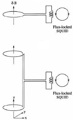
September 8, 2010 10:53 World Scientific Review Volume - 9.75in x 6.5in ch9
160 J. Clarke
(a)
(b)
Fig. 9. Flux transformers. (a) Magnetometer and (b) first-derivative axial
gradiometer, wound from niobium wire. Typical diameter of pickup loops is 50 mm.
quantization — and thus a flux in the SQUID. The transformer operates
at frequencies down to zero. The transformer is optimized when the induc-
tances of the pickup and input coils are equal. For a pickup loop diameter
of 50 mm, a magnetic field noise of 10
−15
THz
−1/2
is typical. Figure 9(b)
shows a first-derivative, axial gradiometer in which the two pickup loops,
nominally equal in area, are wound in opposite senses. Application of a
uniform magnetic field along the axis of the loops produces no net flux in the
transformer and no output from the SQUID. An applied gradient ∂B
z
/∂z,
on the other hand, produces a current in the flux transformer and an output
from the SQUID. Second-derivative axial gradiometers measuring ∂
2
B
z
/∂z
2
and off-diagonal gradiometers sensitive to, for example, ∂B
z
/∂x are also
commonly used. Gradiometers are mostly used to discriminate against
distant noise sources in favor of nearby signal sources: noise from a dipole
falls off with distance r as 1/r
4
and 1/r
5
for first- and second-derivative
gradiometers. Gradiometers are commonly used to measure signals from the
brain (Sec. 8).
6. A Little Theory
The early development of both dc and rf SQUIDs was largely a “seat of
the pants” affair, without any detailed theory to guide their optimization.
