Buschow K.H.J. (Ed.) Concise Encyclopedia of Magnetic and Superconducting Materials
Подождите немного. Документ загружается.

where K
d
¼(1/2)m
0
(N
>
N
8
)M
2
s
. The parameter a
c
,
defined as a
c
¼H
N
(c)/H
N
(0), is shown in Fig. 5 for
the extended theory with K
2
a0 for the case of
Nd
2
Fe
14
B and K
d
¼0 (sphere). Also shown in Fig. 5
are the coercive fields which for c
0
op/4 coincide
with the nucleation fields, but decrease for c
0
4p/4,
because nucleation takes place in the third quadrant.
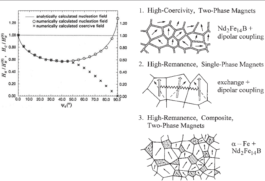
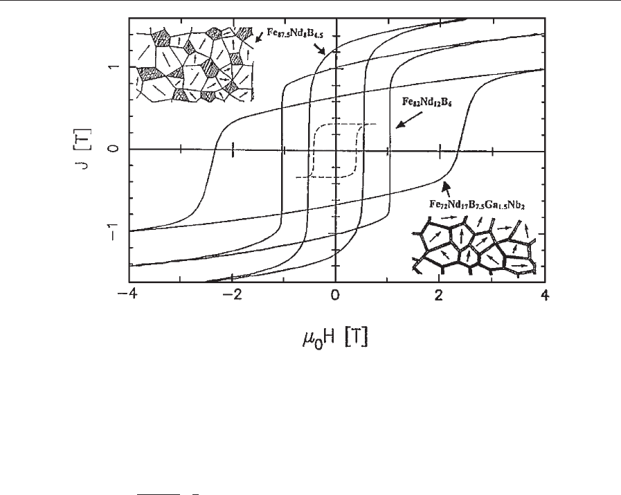
4. Coercive Fields of Assemblies of Grains
In the case of assemblies of grains three types of per-
manent magnets have to be distinguished that are
characterized by special microstructures, as shown
schematically in Fig. 6 and leading to hysteresis loops
presented in Fig. 7:
(i) High-coercivity PMs where the grains are mag-
netically decoupled by a paramagnetic intergranular
film. In the case of R
2
Fe
14
B-based magnets, this
microstructure is realized by an overstoichiometry of
R and suitable additives such as gallium and niobium
(Kronmu
¨
ller et al. 1996) (see Magnets: Sintered).
There still exists a long-range dipolar interaction be-
tween the grains, which, however, becomes rather
small in the case of nanograins (Rieger et al. 1999).
(ii) High-remanence–high-coercivity PMs are ob-
tained if nanograins are magnetically coupled by ex-
change interactions (Kneller and Hawig 1991,
Kronmu
¨
ller et al. 1996). These types of PMs are re-
alized by highly stoichiometric alloys.
(iii) Composite high-remanence PMs (Coehoorn
et al. 1988, Bauer et al. 1996, Goll et al. 1998, Neu
et al. 1996) are obtained by melt-spinning of alloys
with overstoichiometric content of a-Fe. In this
case, in addition to the effect of exchange coupling
between the grains, the large magnetization of a-Fe
also enhances the remanence (see Magnets: Reman-
ence-enhanced).
4.1 Isotropic Distribution of Decoupled Grains
In the case of decoupled grains, a
c
has to be replaced
by an effective value, a
eff
, which takes care of the fact
that the demagnetization process takes place by irre-
versible nucleation processes and also by reversible
rotational processes. Owing to the angular depend-
ence of a
c
all those grains oriented symmetrically
around c
0
¼p/4 reorient their magnetization first.
Neglecting the reversible rotations in the remaining
grains the demagnetization to zero polarization is
performed by those grains with misalignment angles
in the range 301oco601. In this range the average,
/a
c
S, is of the order of 0.53, i.e., this value is very
near to the minimum value a
min
c
¼0.5 at c
0
¼p/4. The
value of 0.53 is even lowered if the contributions of
the reversible rotations are taken into account. Con-
sequently, in the case of an isotropic distribution of
Figure 5
Angular dependence of the nucleation and the coercive
field of a Nd
2
Fe
14
B sphere in reduced units (a
c
¼H
N
/
H
(0)
N
).
Figure 6
Schematic microstructures of nanocrystalline melt-spun
permanent magnets.
70
Coercivity Mechanisms
easy axes, it is a reasonable approximation to use for
a
c
the minimum value a
min
c
, given by (Kronmu
¨
ller
1990)
a
min
c
¼
K
1
þ K
2
2K
1
D
1
2
ð11Þ
4.2 Isotropic Distribution of Exchange-coupled
Grains
In nanocrystalline PMs with exchange coupling be-
tween the grains the coercive field is in general smaller
as compared to exchange-decoupled grains. Several
sources may contribute to this decrease of H
c
. The
random anisotropy effect (Herzer 1990) leads to a
reduction of the effective anisotropy constant if the
grain sizes are smaller than the wall width. In the case
of hard magnetic materials, d
B
o5 nm holds whereas
in most nanocrystalline PMs D is larger than d
B
(10–
20 nm) and therefore the random anisotropy effect
becomes ineffective. Another source of reduced co-
ercive fields are grains with misalignment angles
c
0
4p/4. According to Fig. 5 the coercive field of
these grains decreases to zero for c
0
¼p/2 where
H
N
4H
c
, i.e., they contribute to the demagnetization
process only by reversible rotations.
Owing to the exchange coupling these strongly
misaligned grains increase the rotation of J
s
within
the neighboring grains which leads to an enhance-
ment of the reversal of magnetization in these neigh-
boring grains because the critical angle, j
N
,is
achieved at lower fields. The demagnetization proc-
ess of exchange-coupled grains therefore is a collec-
tive process where a cluster of grains becomes
reversed by the grain of largest misalignment. It can
therefore be assumed that the demagnetization proc-
ess in assemblies of exchange-coupled grains is gov-
erned by the grains with misalignment angles p/
4ocop/2. The average coercive field of these grains
is of the order of (1/4)(2K
1
/J
s
), i.e., a
ex
B1/2.
5. Analysis of Temperature Dependence
5.1 The Nucleation Model
The analysis of hardening mechanisms and of the
temperature dependence of H
c
starts from Eqn. (2).
In general it is assumed that the grains with the
smallest H
c
values determine the global H
c
, i.e., the
grains that are characterized by a
min
c
of Eqn. (11). A
precise value of a
min
c
including K
2
has been deter-
mined by Martinek and Kronmu
¨
ller (1990). With
H
min
N
¼a
min
c
H
N
, Eqn. (2) may be written as
m
0
H
c
¼ a
K
a
ex
m
0
H
min
N
N
eff
J
s
ð12Þ
Figure 7
Hysteresis loops of nanocrystalline PMs with the microstructures of Fig. 6. The broken curve represents the
conventional (Ba, Sr)-based ferrite. The intermediate loop results from the stoichiometric Nd
2
Fe
14
B.
71
Coercivity Mechanisms
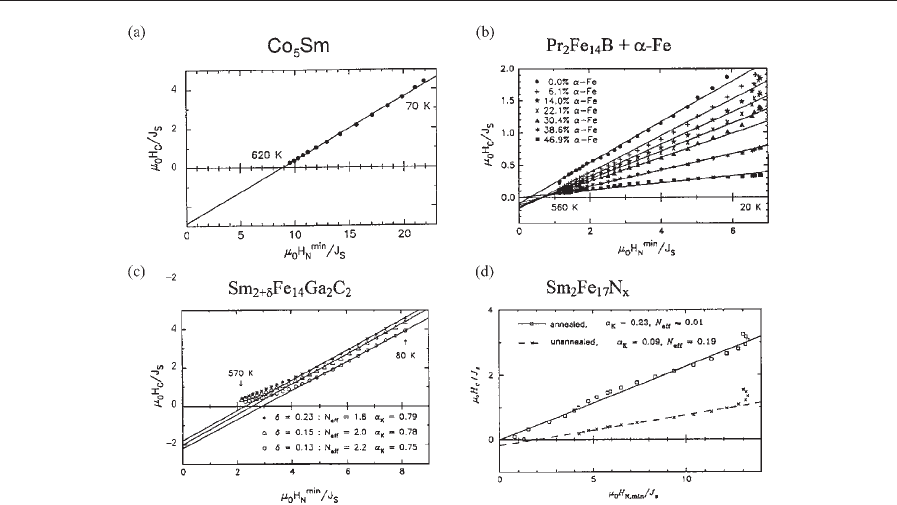
from which it is possible to derive the plot
m
0
H
c
ðTÞ=J
s
ðTÞ7
exp
vs: m
0
H
min
c
ðTÞ=J
s
ðTÞ7
theor
ð13Þ
The left-hand side represents the experimental and
the right-hand side the theoretical values. In the case
of a linear plot the parameters a
K
a
ex
and N
eff
are
obtained as the slope and the ordinate intersection of
the straight line, respectively. These parameters have
been determined for a large number of rare-earth-
based PMs. Figure 8 shows the m
0
H
c
(T)/J
s
(T) plots
for sintered Co
5
Sm, nanocrystalline Pr
2
Fe
14
B þa-Fe,
Sm
2 þd
Fe
14
Ga
2
C
2
(with d ¼0.0, 0.05, and 0.14), and
the nitride Sm
10.7
Fe
89.3
N
x
. In all cases a linear rela-
tionship is found with minor deviations in the case of
the carbide, because the determination of H
min
N
suffers
from a large error in K
1
and K
2
at high temperatures.
The results presented so far clearly show that linear
plots of Eqn. (13) are obtained for nanocrystalline
and sintered PMs. The validity of the nucleation
model therefore seems clear. From the measured a
parameters with the assumption a
ex
¼1/2 for nano-
crystalline and a
ex
¼1 for sintered and decoupled
PMs, values of a
K
are obtained between 0.3 and 0.8,
which corresponds to a width of the inhomogeneity
region of 0.3d
B
o2r
0
od
B
. For example, in the case of
Co
5
Sm with a
K
¼0.33 and a
ex
¼1/2, r
0
is of the order
of 1 nm. Similar results have been obtained previous-
ly for Nd
2
Fe
14
B PMs (Kronmu
¨
ller et al. 1988). An-
other interesting result is the range of a parameters of
nanocrystalline Pr
2
Fe
14
B PMs (Goll et al. 1998). For
decoupled PrFeB PMs with excess praseodymium a
K
values of B0.8 are obtained, whereas the stoichio-
metric exchange-coupled and composite PMs show a
values in the range 0.06–0.32. These small a values of
nanocrystalline PMs are due to the parameter a
ex
,
which reduces the a values by at least 50%. Further-
more, it should be noted that the N
eff
values of sin-
tered magnets are large with N
eff
X1, whereas the
values of nanocrystalline PMs range from 0 to 0.2
because the grains have a spherical shape.
5.2 The Nucleus Expansion Model
Besides the spontaneous nucleation model discussed
in Sect. 5.1 a so-called phenomenological ‘‘global
model’’ has been discussed (Givord and Rossignol
1996). In this model it is assumed that the expansion
of a preformed nucleus takes place by means of a
thermally excited process within the lifetime of the
reversed nucleus that is given by an Arrhenius equa-
tion: t ¼t
0
exp(DE/kt). The pre-exponential factor
is of the order of magnitude t
0
D10
11
s and DE
Figure 8
Plots of m
0
H
c
/J
s
vs. m
0
H
min
N
/J
s
to determine the microstructural parameters a
K
and N
eff
: (a) Co
5
Sm sintered PM;
(b) composite Pr
2
Fe
14
B þa-Fe melt-spun PMs; (c) Sm
2 þd
Fe
14
Ga
2
C
2
carbides with d ¼0.0, 0.05, 0.14; (d)
Sm
10.7
Fe
89.3
N
x
nitride annealed at T
a
¼850 1C for t
a
¼17 min and nitrided at 460 1C.
72
Coercivity Mechanisms
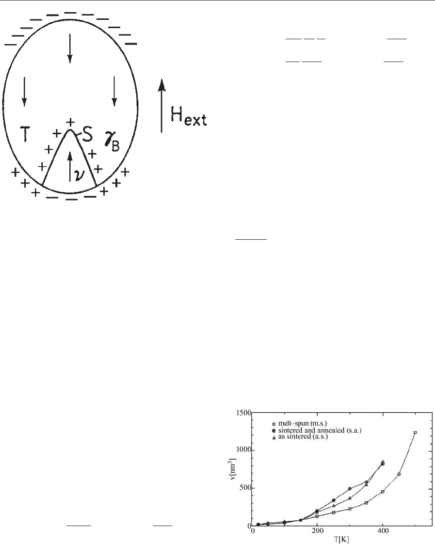
denotes the activation enthalpy required to expand
the nucleus of volume v spontaneously. For usual
measuring times of t ¼110
3
s the activation enth-
alpy DE(t) ¼kTln(t/t
0
) is of the order of DED25kT
(Givord and Rossignol 1996).
The activation energy DE is required in order to
overcome the magnetic enthalpy required for the ex-
pansion of the nucleus. As shown in Fig. 9, at the
coercive field H
c
the three terms of the magnetic
enthalpy are balanced by DE, which leads to
sg
0
B
m
0
M
s
H
c
v m
0
N
eff
M
2
s
v ¼ DE ¼ 25kT ð14Þ
with the domain wall energy, the magnetostatic en-
ergy of the external field at H
c
, and the demagnet-
ization energy. Since it is suggested that the nucleus
is formed in a perturbed region, the specific wall
energy g
B
is reduced as compared to the value of
the perfect crystal, giving g
0
B
¼ a
B
g
0
B
¼ a
B
4
ffiffiffiffiffiffiffiffiffi
AK
1
p
,
where a
B
corresponds to a microstructural parameter
less than unity. The surface, s, of the nucleus may be
related to the volume, v,bys ¼a
s
v
2/3
, where a
s
cor-
responds to a geometrical parameter relating the
nucleus surface to the nucleus volume. From Eqn.
(14), one now obtains
m
0
H
c
¼
a
s
a
B
g
B
M
s
v
1=3
m
0
M
s
N
eff
25kT
vM
s
ð15Þ
Measurements of the activation volume, v, by means
of relaxation curves have shown that v obeys a sim-
ilar temperature dependence as d
3
B
. Therefore, with
v ¼a
3
v
d
3
B
, Eqn. (15) can be rewritten as
m
0
H
c
¼
a
s
a
B
a
v
1
M
s
g
B
d
B
m
0
M
s
N
eff
25kT
vM
s
¼
2K
1
M
s
2a
s
a
B
pa
v
m
0
M
s
N
eff
25kT
vM
s
ð16Þ
Here it becomes obvious that the coercive field of the
global model is described by the same Eqn. (2) or
Eqn. (8) as in the case of the nucleation model. The
only difference seems to be that the nucleation mod-
el is based on the micromagnetic equations whereas
the global model starts from an energetic approach,
i.e., the integrated micromagnetic equations. Since
the thermal fluctuation field m
0
H
f
¼25kT/vM
s
corre-
sponds only to 5–10% of the coercive field, the mi-
cromagnetic energy terms are the dominant ones.
Naturally the fluctuation field can also be introduced
into the nucleation model as a term reducing the
nucleation field. The microstructural parameters a
s
and a
B
can be derived from the plot
H
c
þ H
f
M
s
exp
vs: g
B
=m
0
M
2
s
v
1=3
or vs: m
0
g
B
=J
2
s
v
1=3
ð17Þ
where H
c
, v, and H
f
are determined experimentally
and M
s
and g
B
are obtained from the intrinsic ma-
terial parameters. Figure 10 shows the temperature
dependence of the activation volume of three types
of magnets (melt-spun, sintered and annealed, and
as-sintered). The corresponding plots, according to
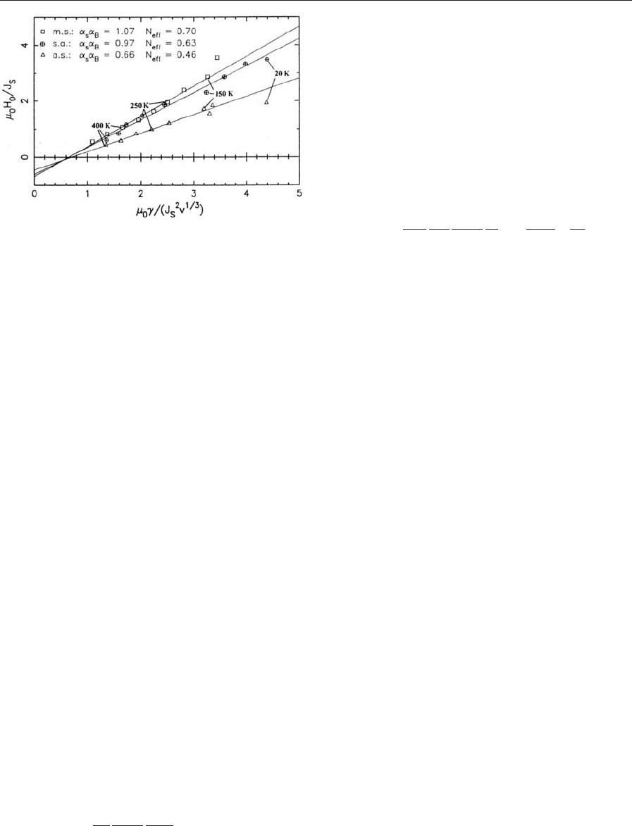
Eqn. (17), are shown in Fig. 11 (Becher et al. 1998).
For all three magnets linear plots are obtained and
the microstructural parameters vary between 0.66
and 1.07. For a nucleus of spherical or conical shape
(apex angle y ¼151) a
s
varies between 4.8 and 2.3. In
the case of the nanocrystalline melt-spun magnet this
means that a
B
varies between 0.2 and 0.4.
Figure 9
Spike-type nucleus of volume v, surface area s, and wall
energy g
0
B
.
Figure 10
Temperature dependence of the activation volume of
three types of magnets.
73
Coercivity Mechanisms
Since the measured activation volumes are of the
order of 300 nm
3
the reduction of the wall energy
should extend over dimensions of B5d
B
(B20 nm).
The problem arising here is the fact that from high-
resolution transmission electron microscopy images
(Kronmu
¨
ller et al. 1996) it is known that the nano-
crystalline grains are perfect with the exception of the
grain boundaries of width 1–3 nm. Accordingly, nei-
ther the values measured for v nor for a
B
are com-
patible with the real microstructure. The situation is
different for the nucleation model where the reversion
of magnetization starts in regions of width 0.5–2 nm
in agreement with the microstructure. Since the glo-
bal theory is just the integrated expression of the
micromagnetic equation, the microstructural para-
meters, a
s
, a
B
, and a
v
may be identified with the
parameters a
K
and a
ex
, i.e., 4a
s
a
B
/pa
v
a
K
a
ex
, which
enlightens one as to the seeming existence of two dif-
ferent theories.
6. Pinning of Domain Walls by Planar Barriers in
Sm
2
Co
17
-based Magnets
Planar defects of atomic width are stacking faults,
phase and antiphase boundaries, and planar precip-
itates as the cell walls of copper-doped Sm
2
Co
17
PMs.
The pinning of domain walls by planar defects has
been treated by the continuum theory of micromag-
netism (Kronmu
¨
ller 1973, Friedberg and Paul 1975,
Hilzinger 1977, Gaunt and Mylvaganam 1981) and
on the basis of the Heisenberg model (Hilzinger and
Kronmu
¨
ller 1975). The pinning effect is due to the
modification of the wall energy by the planar defect.
If the planar defect has extensions larger than the
wall width the coercive field is given by
H
c
¼
1
2J
s
1
cosc
0
dgðzÞ
dz
max
N
eff
M
s
ð18Þ
where dg(z)/dz7
max
denotes the maximum slope of
wall energy. In the case of a linear barrier, dg(z)/
dz7
max
is given by 7g
II
g
I
7/D, where g
I,II
denote the
wall energies in the two neighboring phases and D
corresponds to the width of the defect.
In the case of a narrow defect with Dod
B
the co-
ercive field is determined by the discrete Heisenberg
model (Hilzinger and Kronmu
¨
ller 1975) where the
planar defect is described by its n individual lattice
planes of distance d. Each plane, i, is characterized by
a local anisotropy constant, K
i
, and an exchange
constant, A
i,i þ1
, between neighboring planes. The
result of a lengthy calculation is
H
c
¼
p
3O3
2K
1
J
s
1
cosc
0
d
d
B
X
n1
i¼1
A
A
i;iþ1
K
i
1
K
1
ð19Þ
where A, K
1
, and J
s
are the material constants of the
matrix phase and d
B
is the wall width. Equation (19)
has a wide range of applications and may be applied
for the interpretation of the Sm
2
Co
17
-based magnets
with additives of iron, copper, and zirconium. For
these PMs the largest coercivities of the order of 3–4
T have been found. These hard magnetic properties
are obtained after a homogenizing treatment at
1100–1200 1C (30 min), isothermal aging at 850 1C
(10–25 h), and a subsequent slow cooling (0.5–
1.0 1C min
1
) to 400 1C followed by quenching to
room temperature. During the annealing procedure
a cellular pyramidal structure develops composed
of three phases (Livingston and Martin 1977,
Hadjipanayis 1982): cells of about 100 nm in size
corresponding to an iron-rich 2:17 matrix, cell walls
of SmCo
5
structure separating the cells enriched in
copper and poor in iron and zirconium, and a zirco-
nium-rich lamellar platelet phase, called a Z-phase,
which is oriented perpendicular to the c-axis of the
cells. The cell walls of width 5–10 nm may act as a
barrier or pinning center depending on the copper
content and the degree of order in the 1:5 cell wall. In
the particular case of Sm(Co
bal
Cu
0.08
Fe
0.22
Zr
0.02
)
8.5
Goll et al. (2000) have performed an analysis of the
element distributions within the cells and cell walls by
HRTEM-EDX. The corresponding profile of the
copper and iron distribution and of the anisotropy
constant is shown in Fig. 12 (Goll 2001). The anisot-
ropy constant varies from a value of K
1
2:17
¼
2.9 MJ m
3
to K
1
1:5
¼8.1 MJ m
3
within a narrow
width of B2 nm. Assuming that this increase of near-
ly a factor 3 takes place over 10 atomic layers, where
d ¼0.2 nm and d
B
¼5 nm, m
0
H
c
¼(2K
1
/M
s
) 0.22 is
obtained from Eqn. (19) for a constant exchange en-
ergy. With the a parameter for the pinning a
pin
¼0.22
for room temperature a coercive field of 2.8 T is ob-
tained, in excellent agreement with the experimental
results. Figure 13 shows plots of m
0
H
c
/J
s
vs. 2m
0
K
1
/J
s
2
for different annealing treatments of sintered mag-
nets. Over a wide temperature range between 170 K
Figure 11
Plots for the determination of a
s
a
B
and N
eff
for the
global model of the PMs of Fig. 10.
74
Coercivity Mechanisms
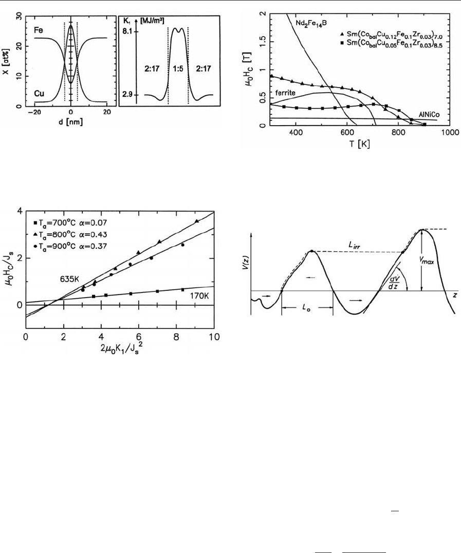
and 635 K a linear relationship is found with a pa-
rameters between 0.07 and 0.43. As is well known
annealing at 800 1C gives the optimal values of the
coercive field. The dominance of the 2:17-based PMs
above 650 K is clearly shown by Fig. 14 where the
coercive fields of several prominent PMs are com-
pared with each other.
7. Statistical Pinning Theory of Domain Walls
In soft magnetic materials based on amorphous,
crystalline, or nanocrystalline alloys the coercive field
is determined by the interaction of domain walls with
a large number of imperfections such as grain bound-
aries, dislocations and point defects, or impurity
atoms. In the case of a dislocation density of
10
10
cm
2
, there are 10
4
dislocations within a domain
wall (DW) of cross-section 10
6
cm
2
. The resulting
force acting on a DW in this case has to be deter-
mined by statistical methods. The force of a defect at
position z
j
acting on a DW at position z is described
by v(zz
j
), where z is the coordinate parallel to the
DW normal. The total force acting on a DW is then
given by (Kronmu
¨
ller 1997)
VðzÞ¼
X
j
vðz z
j
Þð20Þ
where the sum extends over all defects. The statistical
field of force, shown schematically in Fig. 15, is char-
acterized by three parameters:
(i) the average wavelength 2L
0
defined as twice the
distance between neighboring zeros
V(z) ¼0;
(ii) the average value V
max
of the maximum of
V(z); and
(iii) the average of the reciprocal slopes of V(z)at
V(z) ¼0 given by
1=R ¼1=ðdV=dzÞ.
These parameters may be determined by means of
correlation functions under the assumption that the
total forces V obey a Gaussian distribution function
f(V). The probability, f, of finding an interaction
force between V and V þdV or a slope R ¼dV/dz
Figure 12
Copper and iron profiles of the cell wall in
Sm(Co
bal
Cu
0.08
Fe
0.22
Zr
0.02
)
8.5
as measured by high-
resolution EDX transmission electron microscopy and
the corresponding profile of the anisotropy constant.
Figure 13
Plots of m
0
H
c
/J
s
vs. 2m
0
K
1
/J
2
s
for different annealing
treatments of a sintered Sm
2
(CoCuFeZr)
17
PMs
showing the validity of Eqn. (2).
Figure 14
Comparison of the temperature dependence of different
types of PMs showing the dominance of the Sm
2
Co
17
-
type PMs at high temperatures.
Figure 15
Characteristic parameters of the statistical field of force.
75
Coercivity Mechanisms
between R and R þdR is given by
f ðVÞ¼
1
ð2pB
0
Þ
1=2
exp
V
2
2B
0
;
f ðRÞ¼
1
ð2pB
1
Þ
1=2
exp
R
2
2B
1
ð21Þ
The correlation functions B
0
and B
1
are related to the
individual interaction forces, v, by the following in-
tegrals:
B
0
¼
F
B
N
L
3
Z
L
3
=2
L
3
=2
½v
2
ðzÞ/vðzÞS
2
dz
B
1
¼
F
B
N
L
3
Z
L
3
=2
L
3
=2
dvðzÞ
dz
2
(
dvðzÞ
dz
2
)
dz ð 22Þ
where F
B
is the DW area, L
3
the DW distance, and N
the defect density. The characteristic parameters of
the statistical potential are related to the correlation
functions as follows:
2L
0
¼ 2pðB
0
=B
1
Þ
1=2
;
%
V
max
¼ðB
0
=2pÞ
1=2
;
1=R ¼ðp=2B
1
Þ
1=2
ð23Þ
In the following the relationship of the coercive field
is considered. It is given by
m
0
H
c
¼
p
1=2
M
s
F
B
7cosc
0
7
%
V
max
lnL
3
2L
0
1=2
w
0
H
c
M
s
¼7cosc
0
7
p
1=2
2
L
0
L
3
lnL
3
2L
0
1=2
ð24Þ
From Eqns. (23) and (24) the dependence of H
c
and
w
0
on the defect density is obtained as
H
c
p
ffiffiffiffi
N
p
; w
0
p1=
ffiffiffiffi
N
p
ð25Þ
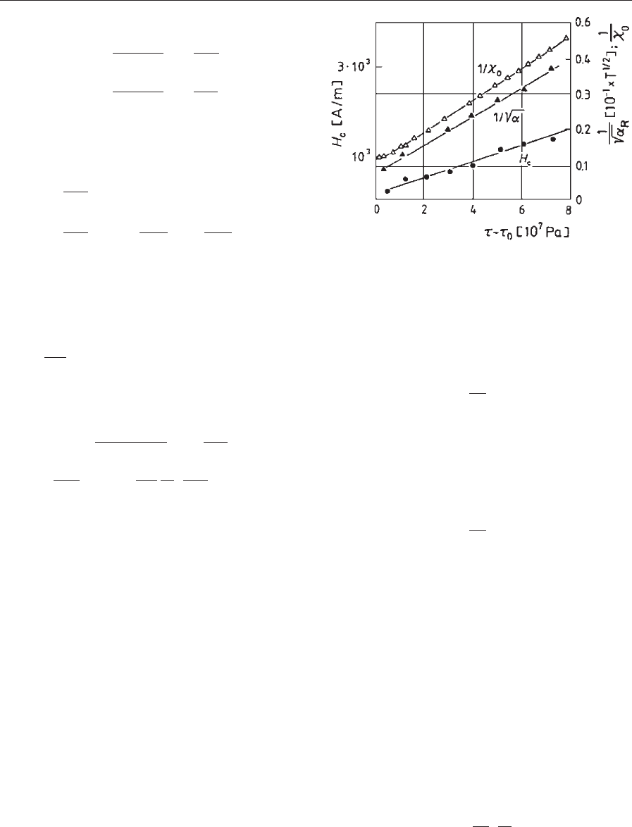
Equation (25) has been tested for plastically de-
formed nickel single crystals where the dislocation
density, N, is related to the applied flow stress, t,by
(Kronmu
¨
ller 1972)
t t
0
¼ 0:36GbðNlÞ
1=2
ð26Þ
where t
0
is the initial flow stress, G the shear mod-
ulus, and l the length of dislocation lines interacting
with the DW. In this case the interaction force is due
to the magnetoelastic coupling energy (Kronmu
¨
ller
1997) and is proportional to the magnetoelastic
stresses of the DW. As a function of the applied
flow stress according to Eqns. (25) and (26) a linear
relationship is expected for H
c
and 1/w
0
as demon-
strated by Fig. 16, which also shows the dependence
of the Rayleigh constant a (Kronmu
¨
ller 1997) fol-
lowing a 1/Np1/(tt
0
)
2
law. Another interesting
feature is the temperature dependence of H
c
, which,
in the case of straight dislocations, is determined by
the intrinsic material parameters M
s
, K
1
, and the
magnetostriction l
s
, and is given by
m
0
H
c
ðTÞp
l
s
M
s
d
1=2
B
pK
1=4
1
ð27Þ
With increasing anisotropy constant K
1
, i.e., de-
creasing wall width d
B
, the pinning strength of dislo-
cations decreases. If one deals with dislocation dipoles
the interaction forces are proportional to the gradi-
ents, rs, of the magnetoelastic stresses of the DW
leading to a temperature dependence of H
c
given by
m
0
H
c
ðTÞp
l
s
M
s
d
1=2
B
pK
1=4
1
ð28Þ
In contrast to the case of individual dislocations, H
c
increases in the case of dislocation dipoles with de-
creasing wall width because this leads to an increase of,
rs, i.e., of the pinning force v. According to Eqn. (28)
the temperature dependence of H
c
follows a K
1/4
1
law
that has been demonstrated to be valid for amorphous
FeNi-based alloys (Kronmu
¨
ller 1997) where the stress
sources correspond to dipole type precipitates of free
volume. The existence of the K
1/4
1
and the K
1/4
1
de-
pendence of H
c
has been found for the case of nickel
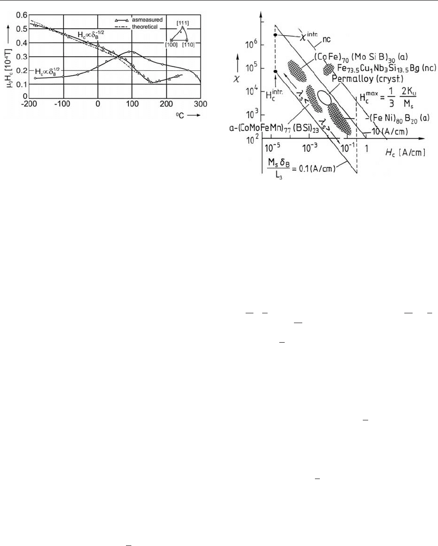
single crystals as shown in Fig. 17. In as-grown nickel
single crystals the main pinning centers are dislocations
leading to the K
1/4
1
law, whereas in neutron-irradiated
single crystals dislocation dipoles exist owing to the
agglomeration of vacancies giving rise to the K
1/4
1
law
for H
c
. H
c
and w
0
are governed by the self-consistency
relationship of Eqn. (24), which may be written as
w
0
D
M
s
H
c
d
B
L
3
ð29Þ
Figure 16
Test of the dependence of H
c
, w
0
, and the Rayleigh
constant, a
R
, on the dislocation density of plastically
deformed single crystals (Kronmu
¨
ller 1972).
76
Coercivity Mechanisms
if one takes into account that the average wavelength,
2L
0
, of the pinning force is of the order of 2d
B
. Owing
to Eqn. (29), w
0
and H
c
may vary only between upper
and lower bounds as determined by the ratio d
B
/L
3
.
This ratio with L
3
B100d
B
–10 000d
B
may vary between
10
4
and 10
2
giving values of 10 A m
1
oM
s
d
B
/
L
3
o10
3
Am
1
for M
s
¼100 kA m
1
. The double log-
arithmic plot of Fig. 18 shows that the CoFe- and
NiFe-based amorphous and crystalline alloys in fact lie
between these two limits, which means that L
3
has
been chosen correctly. Nanocrystalline materials (see
Amorphous and Nanocrystalline Materials)suchas
FeSiNbCuB alloys (Herzer 1990) have a position with
M
s
d
B
/L
3
¼5kAm
1
, which reflects the fact that in
nanocrystalline materials owing to the random anisot-
ropy effect the DW widths are a factor of 5–10 larger
than in amorphous alloys. Figure 18 also includes the
absolute lower and upper limits of H
c
and w
0
, respec-
tively, as expected in ideal amorphous materials with
K
1
-0andl
s
-0 (Kronmu
¨
ller 1981).
8. Computational Micromagnetism of Coercivity
The experimental results for H
c
of hard magnetic ma-
terials show a discrepancy by a factor of 4–5 with re-
spect to the theoretical predictions. In Sects. 2–4 this is
attributed to the role of the microstructure, the effect of
which is described by the microstructural parameters a
and N
eff
. In the case of assemblies of grains, an explicit
calculation of the parameters a and N
eff
is not possible.
Therefore, numerical calculations have been performed
by means of the finite element method (FEM) (Schrefl
et al. 1994). Simulations of magnetization processes of
assemblies of grains start from a minimization of the
magnetic free enthalpy G with respect to the direction
of the spontaneous polarization
J
s
:
dG ¼ d
Z
ðf
A
þ f
K
þ f
s
þ f
H
ÞdV ¼ 0 ð30Þ
The free enthalpy is composed of four contributions:
exchange energy f
A
¼A(rj)
2
, crystal anisotropy
f
K
¼K
1
sin
2
j þK
2
sin
4
j, stray field energy f
s
¼
(1/2)
H
s
J
s
, and magnetostatic energy f
H
¼H
ext
J
s
.
The stray field,
H
s
, follows from a scalar potential
U by H
s
¼rU and U obeys Poisson’s equation
DU ¼m
1
0
div J
s
.
For three-dimensional numerical calculations usu-
ally a cubic particle composed of polyhedral regular
or irregular grains is considered. This model allows
the variation of the average grain size, the modifi-
cation of the magnetic material parameters within
grain boundaries, and the formation of composite
PMs. As an example of the FEM calculations,
Fig. 19 shows the distribution of
J
s
in the remanent
state within a model composite PM of 35 grains with
an average grain diameter of 10 nm with easy axes
distributed isotropically and 51% of soft magnetic
grains of a-Fe, embedded in hard magnetic grains of
Nd
2
Fe
14
B (Fischer et al. 1995). At the grain bound-
aries the direction of
J
s
changes smoothly from one
easy direction to the other within a region of width
2d
B
. Under the assumption of a perfect exchange
coupling between the grains, Fig. 20 illustrates the
dependence of J
r
, m
0
H
c
, and (BH)
max
on the grain
size D for the irregular grains shown in Fig. 19,
and also for a hypothetical regular grain structure of
dodecahedral grains. All three quantities decrease
with increasing grain size and J
r
and H
c
can be fitted
empirically by the following logarithmic laws
Figure 17
Temperature dependence of the coercive field of a nickel
single crystal owing to dislocations (pd
1/2
B
) and to
dislocation dipoles (d
1/2
B
) after heavy neutron
irradiation (xxx ¼3 10
18
ncm
2
) (Kronmu
¨
ller 1966).
Figure 18
Upper and lower bounds for the w
0
vs. H
c
self-
consistency relationship (Eqn. (24)) for crystalline,
nanocrystalline, and amorphous alloys. The upper
bound for w
intr
and the lower bound for H
c
intr
are
obtained for K
1
¼0 and l
s
¼0 (Kronmu
¨
ller 1981).
77
Coercivity Mechanisms
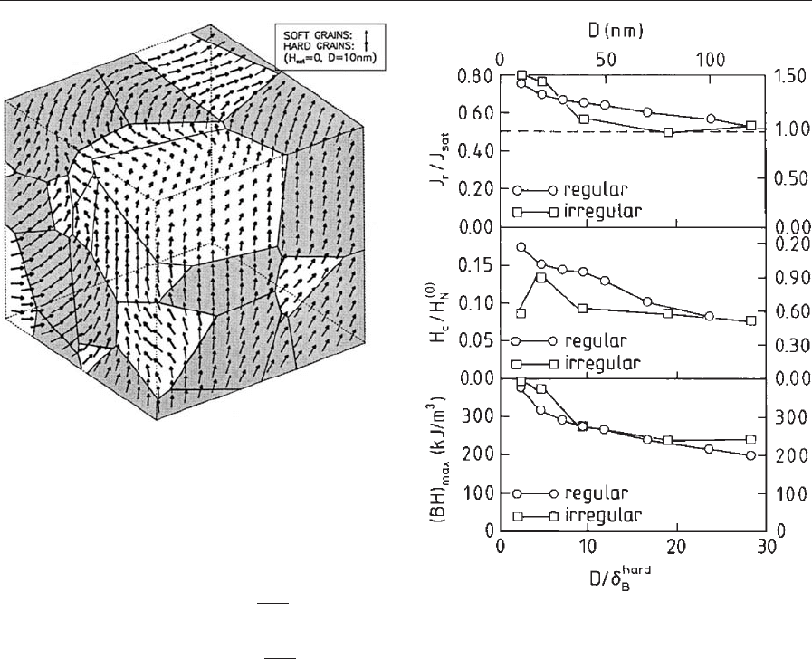
(Fischer et al. 1996):
J
r
¼J
sat
0:84 0:085 ln
D
d
hard
B
!"#
H
c
¼H
ð0Þ
c
0:22 0:041 ln
D
d
hard
B
!"#
ð31Þ
with H
(0)
N
¼2K
hard
1
/J
s
and J
sat
¼J
hard
s
v
hard
þJ
soft
s
v
soft
,
where the superscripts refer to the saturation polar-
izations and volume fractions of the hard and soft
magnetic phases. It turns out that for grain sizes of
20 nm, i.e., 5d
hard
B
, the coercive field is only 15% of
the ideal field H
(0)
N
, and the remanence is consid-
erably larger than the isotropic value of 0.5J
s
.
Figure 21 shows the numerical results for the three
characteristic properties of the hysteresis loops as a
function of the percentage of a-Fe content (Fischer
et al. 1995). Whereas the numerical results for
J
r
agree fairly well with the experimental data, the
theoretical predictions for m
0
H
c
and (BH)
max
are ap-
preciably larger than the experimental values. In
the case of (BH)
max
, this is due to the fact that for
the experimental results the condition m
0
H
c
40.5 J
r
is
only valid for a-Fe concentrations o30% whereas
the numerical results fulfill this condition up to 50%
a-Fe. The observed discrepancy between numerical
and experimental results can be explained by
allowing a modification of the intrinsic material
parameters within the grain boundaries. Owing to
the atomic disorder within a grain boundary it can
be assumed that in particular A and K
1
have reduced
values (Fischer and Kronmu
¨
ller 1996). Figure 22
shows the influence of the reduction of these two
parameters on the demagnetization curve for a cube
of 64 grains of average diameter 20 nm (Fischer and
Kronmu
¨
ller 1998). For the model calculations a
width of 3 nm of the grain boundaries is assumed
where A and K
1
suffer a step-like reduction. With
decreasing A and K
1
within the grain boundaries
m
0
H
c
and J
r
also decrease. If the parameter f ¼A
gb
/
A ¼K
gb
1
/K
1
is introduced where the superscript gb
refers to the grain boundary, H
c
and J
r
obey the
following relationships:
H
c
=H
ð0Þ
N
¼0:304 þ 0:098f
J
r
=J
sat
¼0:646 þ 0:036f ð32Þ
Figure 19
Distribution of polarization within 35 irregular grains of
average diameter 10 nm within a cube with volume
fraction of 51% a-Fe (shaded) and 49% Nd
2
Fe
14
B.
Figure 20
Remanence J
r
, coercivity m
0
H
c
, and maximum energy
product (BH)
max
for the irregular configuration of Fig.
19 and a regular dodecahedral grain structure as a
function of mean grain size D.
78
Coercivity Mechanisms
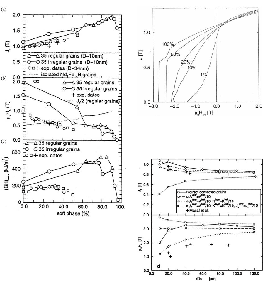
As a further interesting property, the dependence of
the coercive field as a function of the average grain
diameter, /DS, is shown in Fig. 23. Here it turns out
that the experimental results obtained by Manaf et al.
(1991) for nanocrystalline Nd
13.2
Fe
79.6
B
6
Si
1.2
can
only be simulated by the modification of A and K
1
within the grain boundary. Modifications of J
s
lead
to completely controversial results (Fischer and
Kronmu
¨
ller 1996). Figure 24 shows the magnetiza-
tion reversal process for an individual grain sur-
rounded by grains of different easy direction. Here it
is evident that the reversal of magnetization primarily
nucleates within the grain boundaries and the neigh-
boring regions whereas in the bulk of the grain the
magnetization starts to rotate reversibly into the
direction of the applied field.
Figure 21
Numerical results for J
r
, m
0
H
c
, and (BH)
max
of
nanocrystalline composite magnets for regular and
irregular distributions of grains (average grain size
10 nm) as a function of the a-Fe percentage.
Experimental results: þ, Wilcox et al. (1994); J, Bauer
et al. (1996); &, Goll et al. (1998).
Figure 22
Demagnetization curves for an assembly of 64 NdFeB
grains of average grain diameter 20 nm and an
intergranular phase of reduced anisotropy and exchange
constant.
Figure 23
Coercive field as a function of the mean grain diameter
/DS and grain boundaries of reduced material
parameters. The computed points (B) with f ¼0.1
describe the experimental results of Manaf et al. (1991)
fairly well.
79
Coercivity Mechanisms