Bhushan B. Nanotribology and Nanomechanics: An Introduction
Подождите немного. Документ загружается.

14 Mechanical Properties of Nanostructures 757
The SEM images show that below the critical loads the undoped Si(100) and
undopedpolysilicon film were damagedby plowing,associated with the plasticflow
of the material and formation of debris on the sides of the scratch. For the SiC and
SiO
2
films, in regionA, a plowingscratch track was found without anydebris on the
side of the scratch, which is probably responsible for the smoother curve and slower
increase in the coefficient of friction before the critical load. After the critical load,
for the SiO
2
film, delamination of the film from the substrate occurred, followed by
cracking along the scratch track. For the SiC film, only several small debris particles
were found without any cracks on the side of the scratch, which is responsible for
the small increase in the coefficient of friction at the critical load. For the undoped
Si(100), cracks were found on the side of the scratch right from the critical load
and up, which is probably responsible for the big bursts in the friction profile. For
the undoped polysilicon film, no cracks were found on the side of the scratch at the
criticalload. Thismightresult fromgrain boundarieswhichcan stop thepropagation
of cracks. At the end of the scratch, some of the surface material was torn away and
cracks were found on the side of the scratch in the undoped Si(100). A couple of
small cracks were found in the undoped polysilicon and SiO
2
films. No crack was
found in theSiC film. Even at the end ofthe scratch, less debriswas found in theSiC
film. A curly chip was found at the end of the scratch in both Ni
−
PandAufilms.
This is a typical characteristic of ductile metal alloys. The Ni
−
P and Au films were
damaged by plowing right from the beginning of the scratch with material pile-up
at the side of the scratch.
The scratch depth profiles obtained during and after the scratch on all samples
with respect to initial profile, after the cylindrical curvature is removed, are plotted
in Fig. 14.9. Reduction in scratch depth is observed after scratching as compared to
that of during scratching. This reduction in scratch depth is attributed to an elastic
recovery after removal of the normal load. The scratch depth after scratching indi-
cates the final depth which reflects the extent of permanent damage and plowing
of the tip into the sample surface, and is probably more relevant for visualizing the
damage that can occur in real applications. For the undoped Si(100), undoped poly-
silicon film, and SiO
2
film, there is a large scatter in the scratch depth data after the
critical loads, which is associated with the generation of cracks, material removal
and debris. The scratch depth profile is smooth for the SiC film. It is noted that the
SiC film exhibits the lowestscratch depth among the samples examined.The scratch
depths of the undoped Si(100), undoped polysilicon film and SiO
2
film are compa-
rable. The Ni
−
P and Au films exhibit much lager scratch depth than other samples.
The scratch depth of the Ni
−
P film is smaller than that of the Au film.
The critical loads estimated from friction profiles for all samples are compared
in Fig. 14.7 and Table 14.1. The SiC film exhibits the highest critical load of about
14mN, as compared to other samples. The undoped Si(100) and undoped polysi-
licon film show comparable critical load of about 11mN whereas the SiO
2
film
shows a low critical load of about 9.5mN.TheNi
−
P and Au films were damaged
by plowing right from the beginning of the scratch.
758 Bharat Bhushan
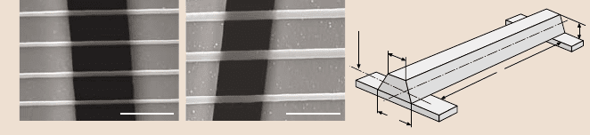
14.3.2 Bending Tests of Ceramic Nanobeams Using an AFM
Bending tests have been performed on Si and SiO
2
nanobeam arrays [62,84]. The
single-crystalsilicon bridgenanobeams werefabricated by bulk micromachiningin-
corporating enhanced-field anodization using an AFM [61]. The Si nanobeams are
oriented along the [110] direction in the (001) plane. Subsequent thermal oxidation
of the beams results in formation of SiO
2
beams.The crosssectionof the nanobeams
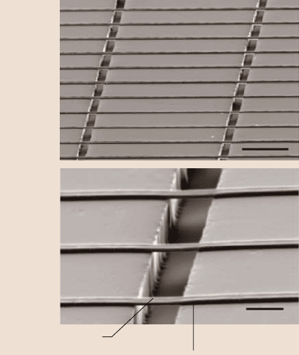
is trapezoidal owing to the anisotropic wet etching process. SEM micrographs of Si
and SiO
2
nanobeam arrays and a schematic of the shape of a typical nanobeam are
shown in Fig. 14.10. The actual widths and thicknesses of nanobeams were meas-
ured using an AFM in tapping mode prior to tests using a standard Si tapping mode
tip (tip radius < 10nm). Surface roughness measurements of the nanobeam surfaces
in tapping mode yielded a σ of 0.7±0.2nm and peak-to-valley (P–V) distance of
4±1.2nmforSiandaσ of 0.8±0.3nm and a P–V distanceof 3.1±0.8nmforSiO
2
.
Prior to testing, the Si nanobeams were cleaned by immersing them in a “piranha
etch” solution (3:1 solution by volume of 98% sulphuric acid and 30% hydrogen
peroxide) for 10minutes to remove any organic contaminants.
Bending Strength
Figure 14.11 shows typical load displacement curves for Si and SiO
2
beams that
were bent to failure [62,84]. The upper width (w
1
) of the beams is indicated in the
figure. Also indicated in the figure are the elastic modulus values obtained from
the slope of the load displacement curve (14.5). All the beams tested showed linear
elastic behavior followed by abrupt failure, which is suggestive of brittle fracture.
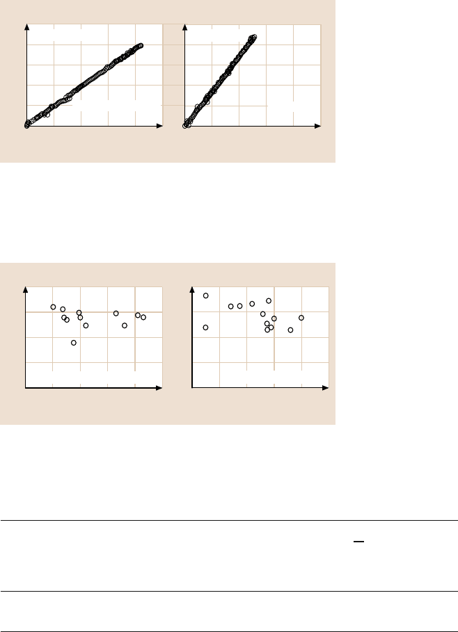
Figure 14.12 shows the scatter in the values of elastic modulus obtained for both
Si and SiO
2
along with the average values (± standard deviation). The scatter in
the values may be due to differences in orientation of the beams with respect to the
trench and the loading point being a little off-center with respect to the beam span.
The average values are a little higher than the bulk values (169GPa for Si[110]
and 73 GPa for SiO
2
in Table 14.2). However the values of E obtained from (14.5)
have an error of about 20% due to the uncertainties in beam dimensions and spring
constant of the tip/cantilever (which affects the measured load). Hence the elastic
modulusvalues on the nanoscale can be consideredto becomparable to bulk values.
w
1
w
2
b)
5 μm
Si SiO
2
5 μm
Neutral axis
a)
l
t
Fig. 14.10. (a) SEM micrographs of nanobeam arrays, and (b) a schematic of the shape of
a typical nanobeam. The trapezoidal cross-section is due to the anisotropic wet etching during
the fabrication [84]
14 Mechanical Properties of Nanostructures 759
100
80
60
40
20
0
2000
Load F
beam
(μN)
400 600 800 1000
Displacement, D
beam
(nm)
E <110> = 189 GPa
w
1
= 295 nm Si
2000
Load F
beam
(μN)
400 600 800 1000
Displacement, D
beam
(nm)
E = 83 GPa
w
1
= 250 nm SiO
2
Fig. 14.11. Typical load displacement curves of silicon and SiO
2
nanobeams. The curves are
linear until sudden failure, indicative of brittle fracture of the beams. The elastic modulus
(E) values calculated from the curves are shown. The dimensions of the Si beam were w
1
=
295 nm, w
2
= 484 nm and t = 255 nm, while those of the SiO
2
beam were w
1
= 250 nm,
w
2
= 560 nm and t = 425 nm [84]
220
190
160
130
100
200100
Elastic modulus E (GPa)
300 400 500 600
Beam upper width w
1
(nm)
E
av
[110] = 182 r 11 GPa
Si
120
90
60
30
0
300200 400 500 600 700
Beam upper width w
1
(nm)
E
av
=85r 13 GPa
SiO
2
Elastic modulus E (GPa)
Fig. 14.12. Elastic modulus values measured for Si and SiO
2
. The average values are shown.
These are comparable to bulk values, which shows that elastic modulus shows no specimen
size dependence [62]
Table 14.2. Summary of measured parameters from quasi-static bending tests
Sample Elastic modulus Bending strength Fracture toughness
E (GPa) σ
b
(GPa) K
IC
(MPa
√
m)
Measured Bulk Measured Reported Estimated Reported Bulk
value (microscale) (microscale) value
Si 182±11 169
a
18±3 < 10
c
1.67±0.40.6–1.65
e
0.9
f
SiO
2
85±13 73
b
7.6±2 < 2
d
0.60±0.20.5–0.9
4
–
a
Si[110] [91]
b
[92]
c
[43,44,46–49,70,93,94]
d
[58]
e
[54–57]
f
[87]
Most of the beams when loaded quasi-statically at the center of the span broke
at the ends as shown in Fig. 14.13a, which is consistent with the fact that maximum
tensile stresses occur on the top surfaces near the ends. (See FEM stress distri-
bution results in Fig. 14.13b.) Figure 14.14 shows the values of bending strength
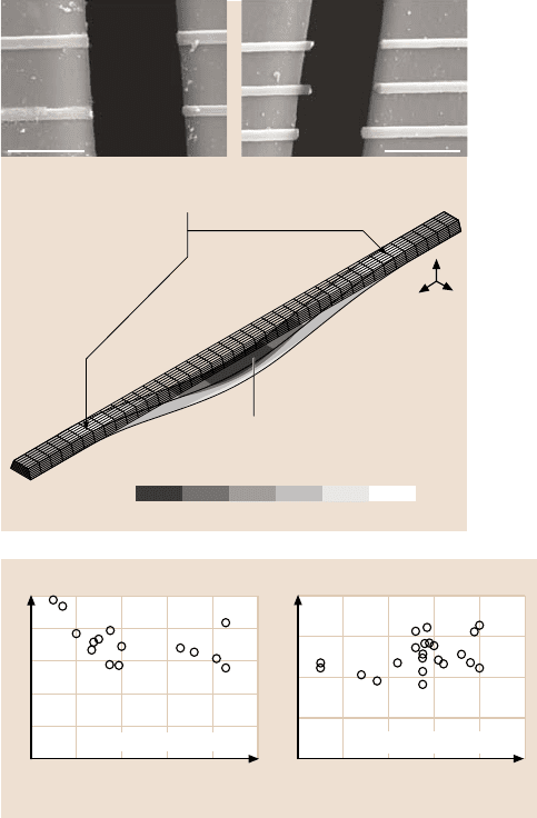
760 Bharat Bhushan
z
x
y
Si SiO
2
a)
Maximum tensile
bending stress
–23 –17 –11 –4 2 9 15GPa
b)
Maximum
compressive stress
5 μm5 μm
Fig. 14.13. (a)SEMmicro-
graphs of nanobeams that
failed during quasi-static
bending experiments. The
beams failed at or near the
ends, which is the location
of maximum tensile bending
stress [84], and (b) bending
stress distribution for silicon
nanobeam indicating that the
maximum tensile stresses oc-
cur on the top surfaces near
the fixed ends
25
20
15
10
5
0
200100
Bending strength σ
b
(GPa)
300 400 500 600
Beam upper width w
1
(nm)
σ
av
= 17.9 r 3 GPaSi
12
9
6
3
0
300200
Bending strength σ
b
(GPa)
400 500 600 700
Beam upper width w
1
(nm)
σ
av
= 7.6 r 1.2 GPa
SiO
2
Fig. 14.14. Bending strength values obtained from bending experiments. Average values are
indicated. These values are much higher than values reported for microscale specimens, indi-
cating that bending strength shows a specimen size effect [62]
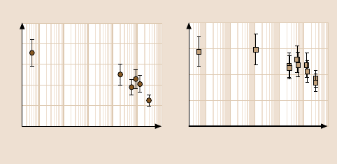
obtained for different beams. There appears to be no trend in bending strength with
the upper width (w
1
) of the beams. The large scatter is expected for the strength
of brittle materials, since they are dependent on pre-existing flaw population in the
material and hence are statistical in nature. The Weibull distribution, a statistical
analysis, can be used to describe the scatter in the bending strength values. The
means of the Weibull distributions were found to be 17.9GPa and 7.6GPa forSi
and SiO
2
, respectively. Previously reported numbers of strengths range from 1–
6 GPa for silicon [44,46–49,51,54,70,93,94] and about 1 GPa for SiO
2
[58] mi-
croscale specimens. This clearly indicates that bending strength shows a specimen
14 Mechanical Properties of Nanostructures 761
2.5
2.0
1.5
1.0
0.5
0.0
0.50.0 1.0 1.5 2.0
Distance from notch tip r
(nm)
Estimated K
IC
(MPa m
1/2
)
Si
SiO
2
Fig. 14.15. Fracture toughness (K
IC
) values of for increasing values of r corresponding to
distance between neighboring atoms in {111} planes of silicon (0.4 nm). Hence r values
between 0.4and1.6 nm are chosen. The K
IC
values thus estimated are comparable to values
reported by others for both Si and SiO
2
[62]
size dependence. Strength of brittle materials is dependent on pre-existing flaws in
the material. Since for nanoscale specimens, the volume is smaller than for micro
and macroscale specimens, the flaw population will be smaller as well, resulting in
higher values of strength.
Fracture Toughness
Estimates of fracture toughness calculated using (14.10) for Si and SiO
2
are shown
in Fig. 14.15 [62]. The results show that the K
IC
estimate for Si is about 1–
2MPa
√
m whereas for SiO
2
the estimate is about 0.5–0.9MPa
√
m.Thesevalues
are comparable to values reported by others on larger specimens for Si [54–57] and
SiO
2
[58].The high valuesobtained for Si could be due to the fact that the scratches,
despite being quite sharp, still have a finite radius of about 100 nm. The bulk value
for silicon is about 0.9MPa
√
m. Fracture toughness is considered to be a material
property and is believed to be independent of specimen size. The values obtained in
this study, given its limitations, appear to show that fracture toughness is compara-
ble, if not a little higher on the nanoscale.
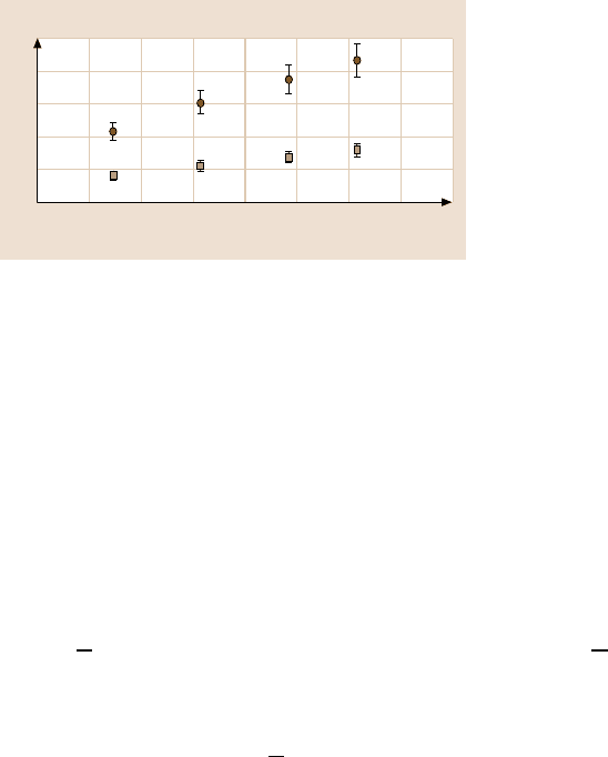
Fatigue Strength
Fatigue strength measurements of Si nanobeams have been carried out by Sun-
dararajanand Bhushan[62] usingan AFM and Li and Bhushan[63] usinga nanoin-
denter. Various stress levels were applied to nanobeams by Sundararajan and
Bhushan [62]. The minimum stress was 3.5GPa for Si beams and 2.2GPaforSiO
2
beams. The frequency of applied load was 4.2Hz. In general, the fatigue life de-
creased with increasing mean stress as well as increasing stress amplitude. When
the stress amplitude was less than 15% of the bending strength, the fatigue life was
greater than 30,000 cycles for both Si and SiO
2
. However, the mean stress had to
be less than 30% of the bending strength for a life of greater than 30,000 for Si
whereas even at a mean stress of 43% of the bending strength, SiO
2
beams showed
762 Bharat Bhushan
25
20
15
10
5
0
10
1
10
0
Bending stress (GPa)
10
2
10
3
10
4
10
5
Number of cycles
> 30k cycles
Si
Bending
strength
12
9
6
3
0
Bending stress (GPa)
Number of cycles
> 30k cycles
SiO
2
10
1
10
0
10
2
10
3
10
4
10
5
Bending
strength
Fig. 14.16. Fatigue test data showing applied bending stress as a function of number of cycles.
A single load–unload sequence is considered as 1 cycle. The bending strength data points are
therefore associated with 1/2 cycle, since failure occurs upon loading [62]
a life greater than 30,000. During fatigue, the beams broke under the loading point
or at the ends, when loaded at the center of the span. This was different from the
quasi-static bending tests, where the beams broke at the ends almost every time.
This could be due to the fact that the stress levels under the load and at the ends
are not that different and fatigue crack propagation could occur at either location.
Figure 14.16 shows a nanoscale S–N curve, with bending stress (S) as a function
of fatigue in cycles (N) with an apparent endurance life at lower stress. This study
clearly demonstrates that fatigue properties of nanoscale specimens can be studied.
SEM Observations of Fracture Surfaces
Figure 14.17 shows SEM images of the fracture surfaces of nanobeams broken dur-
ing quasi-static bending as well as fatigue [62]. In the quasi-static cases, the max-
imum tensile stresses occur on the top surface, so it is reasonable to assume that
fracture initiated at or near the top surface and propagated downward. The fracture
surfaces of the beams suggest a cleavage type of fracture. Silicon beam surfaces
show various ledges or facets, which is typical for crystalline brittle materials. Sili-
con usually fractures along the (111) plane due to this plane having the lowest sur-
face energy to overcome by a propagating crack. However, failure has also been
known to occur along the (110) planes in microscale specimens, despite the higher
energyrequired as comparedto the (111) planes [70]. The plane normal to the beam
direction in these samples is the (110) plane while (111) planes will be oriented at
35
◦
from the (110) plane. The presence of facets and irregularities on the silicon
surface in Fig. 14.17a suggest that it is a combination of these two types of frac-
tures that has occurred. Since the stress levels are very high for these specimens, it
is reasonable to assume that crack propagating forces will be high enough to result
in (110) type failures.
In contrast, the silicon fracture surfaces under fatigue, shown in Fig. 14.17b,ap-
pear very smooth without facets or irregularities. This is suggestive of low energy
fracture, i.e. of (111) type fracture. We do not see evidence of fatigue crack propa-
gation in the form of steps or striations on the fracture surface. We believe that for
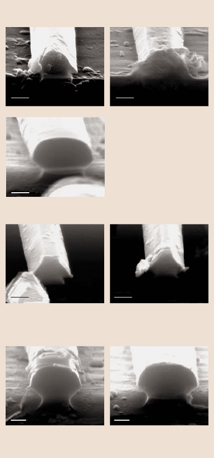
14 Mechanical Properties of Nanostructures 763
a)
b)
Quasi-static bending
Si
200 nm 200
nm
SiO
2
200 nm
Si
Fatigue
SiO
2
200 nm
Fatigue life = 2 k cycles
Mean stress =
8.0 GPa,
stress ampl. = 4.6 GPa
Fatigue life = 0.1 k cycles
Mean stress = 4.8 GPa
stress ampl. = 2.6 GPa
200 nm
200
nm
Si
Si
SiO
2
200 nm
Fatigue life = 13.4 k cycles
Mean stress = 3.7 GPa
stress ampl. = 1.6 GPa
Fatigue life = 6 k cycles
Mean stress = 6.5 GPa
stress ampl. = 3.0 GPa
Fig. 14.17. SEM micrographs
of fracture surfaces of silicon
and SiO
2
beams subjected to
(a) quasi-static bending and
(b) fatigue [62]
the stress levels applied in these fatigue experiments, failure in silicon occurred via
cleavage associated with ‘static fatigue’ type of failures.
SiO
2
shows very smooth fracture surfaces for both quasi-static bending and fa-
tigue. This is in contrast to thehackled surfaceonemight expectfor the brittle failure
of an amorphous material on the macroscale. However, in larger scale fracture sur-
faces for such materials, the region near the crack initiation usually appears smooth
764 Bharat Bhushan
or mirror-like. Since the fracture surface here is so small and very near the crack
initiation site, it is not unreasonable to see such a smooth surface for SiO
2
on this
scale. There appears to be no difference between the fracture surfaces obtained by
quasi-static bending and fatigue for SiO
2
.
Summary of Mechanical Properties Measured Using Quasi-Static Bending Tests
Table 14.2 summarizes the various properties measured via quasi-static bending in
this study [62]. Also shown are bulk values of the parameters along with values re-
ported on larger scale specimens by other researchers. Elastic modulus and fracture
toughness values appear to be comparable to bulk values and show no dependence
on specimen size. However bending strength shows a clear specimen size depen-
dence with nanoscale numbers being twice as large as numbers reported for larger
scale specimens.
14.3.3 Bending Tests of Metallic Microbeams Using a Nanoindenter
Bending tests have been performed on Ni
−
P and Au microbeams [64]. The Ni
−
P
cantilever microbeams were fabricated by focused ion beam machining technique.
The dimensions were 10, ×12, ×50µm
3
. Notches with a depth of 3 µm and a tip
radius of 0.25µm were introduced in the microbeams to facilitate failure at a lower
load in the bending tests. The Au bridge microbeams were fabricated by electroplat-
ing technique.
Figure 14.18 shows the SEM images, load displacement curve and FEM stress
contour for the notched Ni–P cantilever microbeam that was bent to failure [64].
The distance between the loading position and the fixed end is 40 µm. The 3 µm
Ni-P cantilever microbeam
Maximum
tensile
bending
stress
Compressive
Tensile
Load-displacement curve
Broken microbeam
FEM stress contour
at 20 mN
25
20
15
10
5
0
20
Load (mN)
46810
Displacement (μm)
20 μm
5
μm
– 3658 – 843 1970 4785 11599 21671MPa
20 μm
40 μm
10 μm
10 μm
12 μm
Fig. 14.18. SEM micrographs of the new and broken beams, load displacement curve and
FEM stress contour for the notched Ni–P cantilever microbeam [64]
14 Mechanical Properties of Nanostructures 765
deep notch is 10µm from the fixed end. The notched beam showed linear behavior
followed by abrupt failure. The FEM stress contour shows that there is higher stress
concentration at the notch tip. The maximum tensile stress σ
m
at the notch tip can
be analyzed by using Griffith fracture theory as follows [83],
σ
m
≈ 2σ
0
c
ρ
1
2
, (14.11)
where σ
0
is the average applied tensile stress on the beam, c is the crack length,
and ρ is the crack tip radius. Therefore, elastic–plastic deformation will first occur
locally at the end of the notch tip, followed by abrupt fracture failure after the σ
m
reaches the ultimate tensile strength of Ni
−
P, even though the rest of the beam is
still in the elastic regime. The SEM image of the fracture surface shows that the
fracture started right from the notch tip with plastic deformation characteristic. This
indicates that although local plastic deformation occurred at the notch tip area, the
whole beam failed catastrophically. The present study shows that FEM simulat-
ion can predict well the stress concentration, and helps in understanding the failure
mechanism of the notched beams.
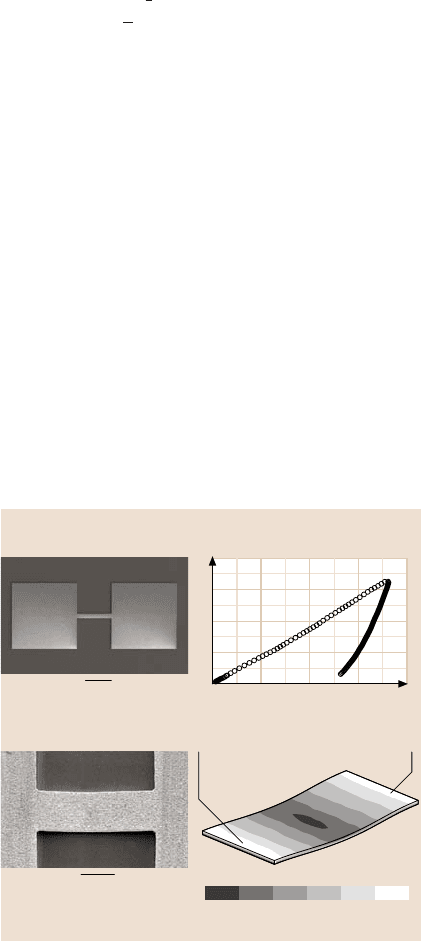
Figure 14.19 shows the SEM images, load displacement curve and FEM stress
contour for the Au bridge microbeam that was deformed by the indenter [64]. The
recession gap between the beam and substrate is about 7 µm, which is not large
enough to break the beam at the load applied. From the load–displacement curve,
we note that the beamexperiencedelastic–plastic deformation.The FEM stress con-
tour shows that the maximum tensile stress is located at the fixed ends whereas the
minimum compressive stress is located around the center of the beam. The SEM
– 956 – 657 – 358 – 60 240 539
MPa
838
Load-displacement curve
4
3
2
1
0
20
Load (mN)
468
Displacement (μm)
Au bridge microbeam
Deformed beam FEM stress contour at 3.2 mN
Compressive Tensile
Maximum tensile bending stress
200 μm
400 μm
Fig. 14.19. SEM micrographs
of the new and deformed
beams, load displacement
curve and FEM stress con-
tour for the Au bridge mi-
crobeam [64]
766 Bharat Bhushan
image shows that the beam has been permanently deformed.No crack was found on
the beam surface. The present study shows a possibility for mechanically forming
the Au film into the shape as needed. This may help in designing/fabricating func-
tionally complex smart micro/nanodeviceswhich need conductorsfor power supply
and input/output signals.
14.3.4 Indentation and Scratch Tests of Polymeric Microbeams
Using a Nanoindenter
Studies have been conducted on two polymer microbeams made of PMMA and
PPMA with thickness of about 2 to 5µm [65]. PPMA was chosen due to its rela-
tively low glass transition temperature, allowing easy thermal processing of the ma-
terial during the microfabrication process. PMMA was chosen due to its wide use
in commercial biomedical applications. Table 14.3 summarizes published data on
these materials.
Hardness and Elastic Modulus
The hardness (H), elastic modulus (E) and creep of PPMA and PMMA beams were
measured at the supported region of the beams [65]. In Fig. 14.20, the indentation
location, where the H, E and creep were measured, is indicated by an arrow. Fig-
ure 14.21ashowsthe H and E of 2.9µm PPMA and 3.4 µmPMMAbeamsasafunc-
tion of contact depth [65]. The H and E were calculated by averaging the H and E
Bending
location
100 μm
20 μm
Indentation location
(H, E, creep)
Fig. 14.20. SEM images of
PPMA beams at low and high
magnifications