Pati S.K., Enoki T., Rao C.N. R. (eds.) Graphene and Its Fascinating Attributes
Подождите немного. Документ загружается.

January 20, 2011 13:57 World Scientific Review Volume - 9in x 6in Chap4
64 A. K. Manna and S. K. Pati
modeled by Sutton-Chen 12-6 potentials.
50
The relative stability of the
metal nanoclusters embedded on graphene surface (i.e., graphene@M
40
)is
determined by the stabilization energies (E
stab
) or the so-called binding
energy, calculated using equation (1). As is well known, the larger the sta-
bilization energy, the stronger is the binding of the guest dopant cluster to
the graphene surface. The stabilization energy per deposited metal cluster
is calculated by subtracting the energy of the optimized isolated cluster of
nuclearity 40, E(M
40
) and the optimized equilibrium energy of the graphene
supercell, E(graphene), from the total energy of the optimized composite
systems, E(graphene@M
40
), :
∆E
stab
= E
graphene@M
40
− E
graphene
− E
M
40
(1)
A summary of the results for the optimized structures for all four com-
plexes is provided in Table 1.
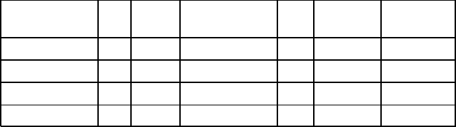
Table 1. Summary of results for metal nanoclusters deposited on graphene. The +ve
(-ve) sign indicates the electron transfer from graphene (metal cluster) to metal clus-
ter (graphene). The R
eq
and C.T represent the equilibrium distances of separation and
amount of charge transfer, respectively. I.E
v
(I.E
a
)andE.A
v
(E.A
a
) represent the verti-
cal (adiabatic) ionization energy and electron affinity, respectively (From reference 45a).
Nanocomposites R
eq
∆E
stab
∆E
form
C.T I.E
v
E.A
v
(
˚
A) (eV) (∆E
form
c
)(eV) (e) (I.E
a
) (E.A
a
)
Graphene@Pd
40
2.33 -4.74 -3.70 (-3.58) 3.62 5.78 (5.76) -3.54 (-3.55)
Graphene@Ag
40
2.45 -2.19 -2.45 (-2.40) 2.00 4.68 (4.68) -2.48 (-2.51)
Graphene@Pt
40
2.35 -2.86 -6.14 (-6.07) 2.41 6.82 (6.60) -4.10 (-4.03)
Graphene@Au
40
2.83 -1.91 -4.13 (-4.03) -0.17 4.10 (4.10) -1.49 (-1.54)
We too have calculated the formation energies (E
form
) per metal atom
defined by equation (2) and (3) of these metal nanoclusters in presence as
well as in absence of graphene to focus on the feasibility of spontaneous for-
mation of clustering from constitutional atomic metal moiety under suitable
experimental conditions. Our results indicate that the formation energy is
slightly increased in presence of graphene, acting as a catalyst, relative to
the free metal clustering.
∆E
form
=[E
graphene@M
40
− E
graphene
− 40 ∗ E
M
40
]/40 (2)
∆E
c
form
=[E
M
40
− 40 ∗ E
M
]/40 (3)
January 20, 2011 13:57 World Scientific Review Volume - 9in x 6in Chap4
Doping of Graphene: A Computational Study 65
where the E(M
40
) and E(M) are the energies of optimized metal nanocluster
and of a single metal atom, respectively.
From the fully optimized geometries, we find that the shortest separa-
tion between a metal atom of the deposited metal cluster and the closest
carbon atom of the graphene layer for the graphene@M
40
complexes are
between 2.3 and 2.8 (see Table 1). Also as given in table 1, the rela-
tive stabilization energies are higher in magnitude for Pd, Ag, Pt clusters
embedded graphene complexes compared to the Au
40
cluster which clearly
indicates a relatively weak interaction between the Au nanoparticles and
the graphene in comparison to others. The relatively higher binding ener-
gies combining with smaller equilibrium distances of separation dictate that
all three (Pd, Ag, Pt) metal clusters do eventually adsorbed strongly on
the graphene surface, inducing local structural deformation. An analysis of
the M¨ulliken population suggests that there is an effective charge transfer
between the adsorbed metal cluster and graphene. For the Pd, Ag, and Pt
cluster deposition, the charge transfer occur from graphene to metal cluster
at their equilibrium distances of separation, while for Au nanoclusters the
direction of charge transfer is from metal cluster to graphene. It is also
clear from the table 1 that the extent of charge transfer for Pd, Ag, Pt
nanocluster is larger compared to that for the Au cluster with greater ex-
tent of charge transfer for Pd case, resulting in higher stabilization energy.
To understand this, we have computed the vertical as well as adiabatic
first ionization energy (I.E.) and electron affinity (E.A.) of individual metal
clusters. Both the I. E. and E. A. values computed with the two differ-
ent strategies follow the similar trend and can be analyzed to understand
the extent of charge transfer. We find that the trend in extent of charge
transfer which determines the overall stabilization energy of the complexes
follow the same pattern in changes in either I. E. or E. A. of the metal clus-
ters belonging to a particular period in the periodic table. In contrast to
Pd, Ag, Pt clusters, the comparatively smaller magnitude of E. A. together
with relatively lower value of I. E. make the Au
40
cluster to act as weak
electron donor towards the graphene.
In order to understand the mechanism and the extent of charge trans-
fer, we have calculated the energy and difference in charge densities of
the composites by varying the distance between the ad metal nanoclus-
ters and the graphene. The interaction energy is found to change inversely
with the distance between metal cluster and graphene, clearly predicting
that such interactions are mainly due to Coulombic forces as already ob-
served for SWCNT interacting with Pt, Au nanoclusters
51
and for electron
January 20, 2011 13:57 World Scientific Review Volume - 9in x 6in Chap4
66 A. K. Manna and S. K. Pati
donor/acceptor adsorbed SWCNT
52
and graphene cases.
45
From the anal-
ysis of difference in charge density, we also find that the electron density at
the outermost valence orbitals of Pd, Ag, and Pt increases while that at the
orbitals of carbon in closer proximity to the metal cluster decreases. The
situation is exactly reversed for the Au nanoparticle deposition on graphene
as expected from the reverse directionality of charge transfer. Thus, our re-
sults predict that the changes in electronic properties of nanoclusters doped
graphene is mainly due to direct charge transfer between the two.
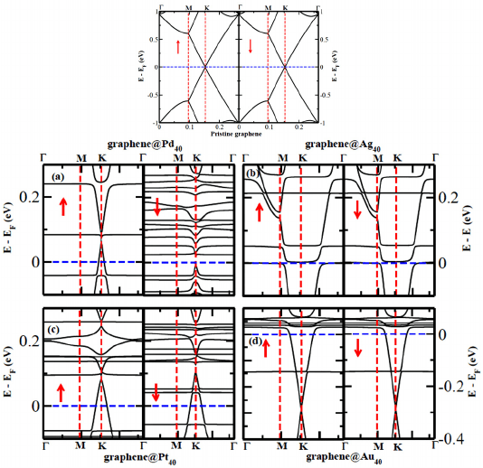
We consider to focus on the changes in electronic band structures of the
metal nanoclusters embedded graphene systems. From the fully relaxed
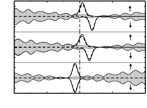
configuration of all the nano composites, it is clear from Fig. 2 that the
region of the graphene in close proximity to the metal cluster is slightly
deformed for all the metal clusters deposition which is capable of breaking
Fig. 2. (Color online) The electronic band structures of pristine graphene (top pannel)
and of four metal nanoclusters embedded nanocomposites (bottom pannel). The energy
is scaled with respect to the Fermi Energy (E
F
). The up and down arrows indicate the
majority and minority spin channel, respectively (From reference 45a).
January 20, 2011 13:57 World Scientific Review Volume - 9in x 6in Chap4
Doping of Graphene: A Computational Study 67
the local A-B sublattice symmetry. Consequently, this can indeed cause
an opening of band gap in the charge transfer complexes near the Fermi
energy. Interestingly, we find that the band gap of a few meV opens near to
the K-point, between the graphene-like bands which touches at the Dirac
point in case of pure graphene, as can be seen from Fig. 2. The effect is
very negligible for Au
40
intercalated graphene as expected from small struc-
tural changes mentioned above. It is also to be noted that the energy-gap
region is above (below) the Fermi energy due to electron transfer from the
graphene (metal nanoclusters) to metal nanoclusters (graphene) for Pd, Ag,
Pt (Au) and, therefore, the neutral systems are still metallic. The appropri-
ate tuning of carriers concentration can result in placing the Fermi energy
in the gap region, and the resulting system would behave as semiconductor.
However, all the bands for composite systems are essentially a superposi-
tion of the bands arising from isolated systems. Moreover, the flat bands
near the Fermi level arise from the localized electronic states of the metal
nanoclusters, whereas the bands at the high symmetric K-points are mainly
from graphene. The calculated density of states (DOS) and its projection
on individual fragment present in nanocomposites show that the graphene
is indeed still in its semi-metallic state for the deposition of nanoclusters
Pd
40
and Pt
40
, while the same becomes metallic in presence of metal nan-
oclusters Ag
40
and Au
40
. The relatively strong adsorption of Pd
40
and Pt
40
nanoclusters on graphene induced by the larger extent of charge transfer
result in a net spin polarization for the complexes. The spin-polarization
of the two nanocomposite arises mainly from the adsorbed metal clusters.
Interestingly, the graphene@Pd
40
nanocomposite can act as perfect spin
filter without any charge injection as can be seen from Fig. 2(a). This is
because of the presence of metallic majority spin channel, whereas the mi-
nority spin channel is semiconducting, i.e., typical half-metallic behavior.
Therefore, the doping of appropriate metal cluster on 2D graphene shows a
new inroads towards designing of new nanomaterials of tunable electronic
properties including room temperature half-metallicity for advanced device
applications.
4. Molecule-Graphene Complexes
In this section, we discuss the changes in opto-electronic properties of 2D
graphene induced by molecular charge transfer.
45
To achieve the goal, we
have considered a few representative organic donor and acceptor molecules.
The schematic diagram of which is shown in Fig. 3.
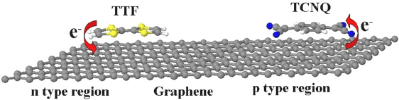
January 20, 2011 13:57 World Scientific Review Volume - 9in x 6in Chap4
68 A. K. Manna and S. K. Pati
Fig. 3. Schematic representation of charge transfer process between graphene and elec-
tron donor, TTF and electron acceptor, TCNQ molecules. The yellow, blue, grey, and
white color atoms correspond to sulfur, nitrogen, carbon and hydrogen, respectively
(From reference 45b).
From the relaxed geometries, we find that all the sorbed molecules sur-
face adsorbed above the graphene at about 3.0
˚
A.
45
Moreover, the calcu-
lated adsorption energies that essentially examine the relative stability of
adsorbate-graphene complexes are within a few kcal mol
−1
(30 - 50 kcal
mol
−1
), suggesting a physisorption process
45
with larger adsorption en-
ergy for TCNQ adsorbed complex. An analysis of the M¨ulliken population
suggests that there is an effective charge transfer between the adsorbed
molecule and graphene. For both TCNE and TCNQ, the extent of electron
transfer from graphene to adsorbed molecule is found to be ∼ 0.31 e and
∼ 0.39 e, respectively, consistent with their nature of electron-withdrawing
tendency.
45
For electron donor, TTF, electron transfer of ∼ 0.11 e is found
from the molecule to graphene. The large value of adsorption energy for
TCNQ on graphene compared to the others can be attributed to the fact
that for TCNQ, the benzenoid structure provides a significant π surface for
adsorption on graphene with a significant amount of charge transfer, and
gains stability through electrostatic forces. Incidentally, the charge transfer
between graphene and adsorbed molecule results in electrostatic attraction
and thereby formation of a charge-transfer complex, in agreement with
the UV/Vis spectrum reported by Rao and co-workers.
43,44
Furthermore,
it is also indentified conclusively that the charge transfer occurs through
Coulombic forces, as was the case for the interaction of carbon nanotubes
with metal nanoparticles
51
and with donor and/or acceptor molecules, and
nanocluster-graphene cases as discussed in previous section.
52
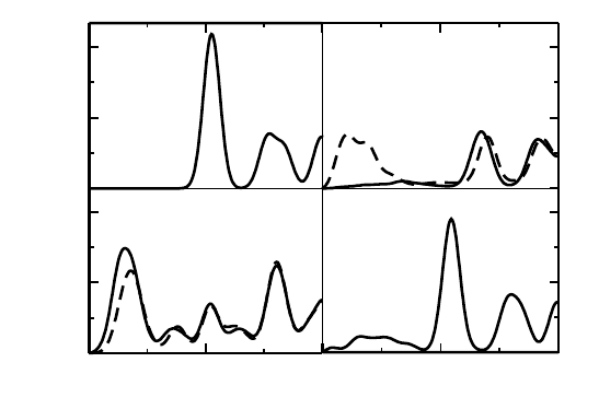
To analyze the effect of charge transfer interaction on electronic struc-
ture, we plot band diagrams and corresponding DOS in Fig. 4. The band
structures around the Dirac point are significantly affected by molecular
adsorption in graphene. For pristine 2D graphene, spin-polarized DOS
vanishes exactly at Fermi level due to the presence of massless Dirac
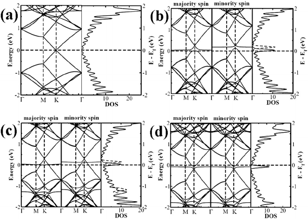
January 20, 2011 13:57 World Scientific Review Volume - 9in x 6in Chap4
Doping of Graphene: A Computational Study 69
Fig. 4. The band structure and corresponding DOS for (a) pure Graphene, (b)
Graphene-TCNE, (c) Graphene-TCNQ and (d) Graphene-TTF in the 8×8 supercell.
The solid and dashed lines in DOS correspond to the majority and minority spins re-
spectively. The Fermi level is set to zero. The DOS lines are broadened with Gaussian
functions of width 0.05 eV (From reference 45b).
fermions and there is no net spin-polarization (see Fig. 4(a)). The cal-
culated DOS and band structures of graphene in presence of donor and
acceptor molecules clearly show the presence of discrete molecular levels
around the Fermi energy. The flat molecular levels of TCNE and TCNQ
in charge-transfer physisorbed systems at slightly above the Fermi level
causes depletion of electrons from the uppermost valence bands, shifting
the Fermi level down. In case of TTF adsorbed graphene, a flat band
slightly below the Fermi level results in accumulation of electrons causing
the upward shifting of the Fermi level, giving rise to finite DOS close to the
Fermi level.
45
Also note that, in all three molecule-graphene complexes,
breaking of the A-B sublattice symmetry induced by the local structural
deformation creates a small band-gap. Injecting either electrons or holes
can indeed change the electronic state from semi-metallic to metallic and
even to a semiconducting state by placing the Fermi level in between the
gap region. Note that, in a strict sense, the Dirac cone picture of graphene
is absent in graphene-molecule complexes. Instead, as shown in Fig. 4, the
January 20, 2011 13:57 World Scientific Review Volume - 9in x 6in Chap4
70 A. K. Manna and S. K. Pati
-8
0
8
-8
0
8
Projected Density of States
-1
-0.5
0
0.5
1
E - E
f
(eV)
-8
0
8
(a)
(b)
(c)
Fig. 5. The projected density of states (pDOS) for (a) Graphene-TCNE, (b) Graphene-
TCNQ and (c) Graphene-TTF in the 8×8 supercell. The Fermi level is set to zero. The
solid, dashed lines and filled dotted areas correspond to total DOS, molecule pDOS and
graphene pDOS respectively. The DOS lines are broadened with Gaussian functions of
width 0.05 eV (From reference 45b).
mixing of graphene band and discrete molecular level results in disappear-
ance of cone picture for valance band for TCNE and TCNQ and conduction
band for TTF. Interestingly, for electrochemical top-gating study, the lin-
ear dispersion near the Fermi level (cone picture) remains true even after
doping to a high level.
36–38
In our case,
45
as has been mentioned, the
charge-transfer is molecular in nature unlike the electrochemical gating.
From the pDOS analysis (see the Fig. 5), it is clear that the DOS at
the Fermi level mainly comes from the adsorbed molecules. In fact, the
graphene in graphene-molecule complex contributes only a little to the
overall DOS at the Fermi energy. Note that, for pure graphene, there
is no states at Fermi energy for transport process. It is also clear from
Fig. 5 that at Fermi energy, a finite spin polarization exists for TCNE and
TCNQ complexes with graphene, while for TTF adsorbed graphene such a
spin polarization is absent.
Here, we also discuss about the Raman active bands (G and D) of
graphene and graphene-molecule complexes for a direct comparison and
detail understanding of the experimental results recently reported by Rao
et al.
43,44
Experimentally, it was shown that G-band softens and stiffens
January 20, 2011 13:57 World Scientific Review Volume - 9in x 6in Chap4
Doping of Graphene: A Computational Study 71
with increasing concentration of TTF and TCNE, respectively, with en-
hancement of the intensity ratio of D- to G-band.
44
In our calculations,
45
we have obtained qualitatively similar results. For pure 2D graphene, our
calculations yield the optical phonon frequency at Brillouin zone center
Γ-point corresponding to the Raman active G-band at around 1579 cm
−1
.
However, in presence of electron acceptors (TCNE and TCNQ), we find that
the G-band frequency is shifted to a higher value (∼ 1599 cm
−1
and ∼ 1596
cm
−1
for TCNE- and TCNQ-adsorbed graphene, respectively) because of
the nonadiabatic removal of Kohn anomaly at Γ-point, while for the elec-
tron donor (TTF), it goes to a lower frequency region at about 1565 cm
−1
,
corroborating the experimental findings.
43,44
We also find that in presence
of strong electron acceptors like TCNE and TCNQ, the intensity ratio of
D- to G-band increases three orders of magnitudes (∼ 10
3
), while for TTF
adsorption, the intensity ratio increases only to two orders of magnitude
(∼ 10
2
), smaller than that for strong acceptors as found experimentally.
43,44
We find reasonably good agreement with previous calculations
53,54
and ex-
perimental results.
43,44,55
To compare and contrast the low frequency optical excitations which can
be affected by molecular charge transfer, we plot the low frequency regime
of the optical conductivity for pure graphene along with donor ( TTF) and
acceptor (e.g; TCNE, TCNQ) intercalated graphene in Fig. 6. Note that,
for pure 2D graphene, the Fermi level lies exactly at Dirac point resulting
in only the possibility of inter band electronic transitions, giving rise to
the optical conductivity peak only at above 0.50 eV. However, for molecule
adsorbed on graphene, the shifting of Fermi level towards the valence band
or conduction band from the Dirac point depending on the nature of the or-
ganic dopant as discussed earlier, creates the possibility of Drude like intra
band transitions, resulting in the low frequency optical excitation below
0.50 eV.
45
This can also be accounted for the appearance of flat molec-
ular levels in between the valence and conduction bands. Interestingly,
the significant amount of charge transfer for TCNE- and TCNQ-adsorbed
graphene induces spin-polarization effects on low-frequency optical conduc-
tivity profile. In fact, this induces asymmetry to the population of majority
and minority spins at the Fermi level (see Fig. 4), which result in the differ-
ence in conductivity values for the carriers with different spins in the low
frequency region (see Fig. 6). However, for TTF-adsorbed graphene, due
to comparatively less charge transfer, both the majority and minority spins
show symmetric population (see Fig. 4), with less intense low-frequency
peaks in optical conductivity.
January 20, 2011 13:57 World Scientific Review Volume - 9in x 6in Chap4
72 A. K. Manna and S. K. Pati
0 0.5
1
150
300
0.5
1
150
300
0
0.5
1
150
300
0.5
1
150
300
σ
1
/(Ω cm)
-1
ω/(eV)
(a)
(b)
(c)
(d)
Fig. 6. Low frequency optical conductivity for (a) pure Graphene, (b) Graphene-TCNE,
(c) Graphene-TCNQ and (d) Graphene-TTF. The solid and dashed lines in conductiv-
ity profiles correspond to the majority and minority spins respectively. The lines are
broadened with Gaussian functions of width 0.05 eV (From reference 45b).
5. Summary
In this chapter, we have presented emerging results on the effect of external
doping induced by the deposition of a few metal clusters and donor/acceptor
molecules in the modification of the intriguing electronic structure of pris-
tine 2D graphene using first-principles density functional theory level of
calculations. Our results show that the nature of the external dopants has
a significant effect in tuning the electronic structure of graphene through
charge transfer mechanisms. The presence of dopant metal clusters opens
up a small band gap between the valence and conduction bands, and thus
offers a possibile semi-metal to perfectly metallic transition. Interestingly,
we find typical half-metallic behavior for graphene@Pd
40
nanocomposite
which has potential applications in spintronic device fabrication. We have
also shown that the presence of organic donor or acceptor molecules on
graphene can significantly change the electronic properties, in particular
the characteristic Raman spectra of graphene. For all cases, the magnitude
of adsorption energies are found to be moderate, suggesting physisorption
process. Similar to the metal cluster dopants, in molecular cases also we
find that there is an effective charge transfer, the signature of which is found
January 20, 2011 13:57 World Scientific Review Volume - 9in x 6in Chap4
Doping of Graphene: A Computational Study 73
experimentally in UV-visible spectra. The stabilization energies are rela-
tively larger for metal cluster dopants compared to the molecular dopants
since it is governed by the extent of charge transfer. As a result, the effect
in changes of the electronic structure is more pronounced for the former
case. We find a downward shift of Fermi level relative to the Dirac point
for TCNE and TCNQ adsorbed graphene, whereas the Fermi level shifts
upward from the Dirac point for TTF intercalated graphene. Moreover, we
have also found that a small band gap opens up in between the valence and
conduction bands, and thus, tuning of carrier concentrations indeed can
change the graphene electronic structure from semi-metallic to a perfect
metallic through semiconducting behavior. Interestingly, we find that the
molecular charge-transfer results in stiffening and softening of Raman ac-
tive G-band frequency depending on the nature of the dopant molecule and
an increase in the intensities ratio of D- to G-band in presence of dopants,
as found experimentally. Thus, the Raman spectra can be used as a fin-
ger print for understanding the molecular charge-transfer interactions in
graphene-adsorbate complexes. We also suggest that these charge-transfer
effects can be seen in optical conductivity profiles as the low frequency
regions are affected by the molecular charge transfer. Since adsorption of
donor or acceptor dopants gives rise to tuning of band-gap as well as carrier
type in graphene, we propose that it is possible to fabricate the graphene-
based electronic devices through simple means, possibly even a p-n junction
using both donor and acceptors.
Acknowledgments
The authors are grateful to Prof. C. N. R. Rao for his endless inspirations
and all time encouragement. A. K. M. acknowledges CSIR, Govt. of India
for the research fellowship and S. K. P. acknowledges the research grant
from CSIR and DST, Govt. of India.
References
1. G. Dresselhaus, M. S. Dresselhaus, P. C. Eklund, Science of Fullerenes and
Carbon Nanotubes: Their Properties and Applications, Academic Press, New
York, (1996).
2. K. S. Nonoselov, A. K. Geim, S. V. Morozov, D. Jiang, Y. Zhang, S. V.
Dubonos, I. V. Grigorieva, A. A. Firsov, Science, 306, 666, (2004).
3. K. S. Nonoselov, D. Jiang, F. Schedin, T. J. Booth, W. Khotkevich, S. V.
Morozov, A. K. Geim, Proc. Natl. Acd. Sci., 102, 10451, (2005).