Microwave Journal 2011 №04
Подождите немного. Документ загружается.

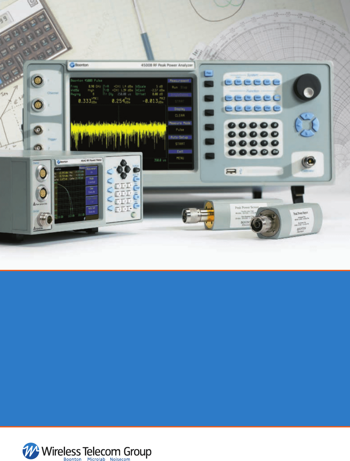
Boonton
Boonton’s Peak Power Meters…
In the past, your options were using one- or two-tone test
signals to measure amplifier linearity. Today, Boonton al-
lows you to use your signal to characterize your DUT. No
more extrapolating graphs or guessing likely compression
points. Our family of peak power meters offers powerful
statistical analysis tools, and is joined by the fastest and
widest dynamic range sensors in the industry.
If you measure extreme signals with:
• High peak to average ratio
• Ultra-low duty cycle
• Noise-like communication signals
Boonton delivers the fastest and most
comprehensive results in the industry.
The Future of Amplifier Testing.
For more information visit us at boonton.com or call
+1 973-386-9696
MWJBOONTON0910.indd 81 3/25/11 2:12 PM
82 MICROWAVE JOURNAL APRIL 2011
Technical FeaT ure
Spinnaker Microwave offers a complete line
of frequency synthesizers including everything from
low cost surface-mount to broadband state-of-the-art
systems. Our design expertise includes: single and multiple
loops, integer and fractional divider schemes, switched
VCO/filter designs, digitally tuned oscillators, frequency
multipliers, integrated up/down converters, direct analog
and DDS-based designs.
• DC to 40 GHz Coverage
• The Most Compact Designs Available
• <1 μsec Switching Speed
• Integrated Phase Noise Down to 0.02 deg RMS
• Low Cost, Lightweight Intergated Module
• Military and Commercial Applications:
Active Jamming, Radar, Communications,
SATCOM, EW, Test Equipment
• Operating Temperature: -45°C to +85°C
• Built for High Vibration Environments
At Spinnaker Microwave, our products are designed with
one thing in mind – your specifications. We pride ourselves
on delivering quality signal sources custom tailored to your
unique application. Contact Spinnaker Microwave today for
the high-performance microwave
sources you can count on.
3281 Kifer Rd, Santa Clara, CA 95051 • Tel: 408-732-9828 • Fax: 408-732-9793 • www.spinnakermicrowave.com
Your compact high-performance
synthesizer solution
Your compact high-performance
synthesizer solution
spinnaker.ads_1/3 pg horz 3/17/11 12:33 PM Page 1
through the network, the impedance
should be transformed from Z
2
to the
exact conjugate match Z
1
*. However,
the transformed impedance is Z
T
,
whose difference from Z
1
* results
in mismatch loss that is exploited to
equalize the gain between the states.
Transformation to the high resistance
region of the Smith chart (E’) is also
necessary for minimum bandwidth.
5
In
addition to the transformation purpose,
the series capacitors (C
1
and C
4
) also
behave as DC blocking capacitors. The
shunt capacitor C
2
is realized by using
four shunt capacitors with FET switch-
es placed in series for frequency control.
Here, the center frequency switching
takes place by varying the capacitance
ance matching network used in the in-
terstage. This network has a bandpass
response. Impedance matching using
a Smith chart was used to determine
the initial components values.
Figure 2 shows the impedance
transformations used to reach the
high-Q contour on the Smith chart.
The series capacitor C
4
transforms the
input impedance of the second-stage
amplifier, Z
2
to A’. The shunt capacitor
C
3
then transforms A’ to B’, the series
inductor L
2
transforms B’ to C’, the
shunt capacitor C
2
transforms C’ to
D’, the shunt inductor L
1
transforms
D’ to E’ and finally the series capaci-
tor C
1
transforms E’ to Z
T
. Ideally,
to ensure maximum power transfer
Circuit Design and
Small-signal
Performance
The first step in the design is the
selection of the first- and second-stage
BJTs, including biasing and ballast net-
works, and input and output matching
for 1 to 2 GHz operation. This initial
design uses simple high-pass and low-
pass L-section matching networks for
the input and output. A blocking ca-
pacitor is used in the interstage and
some resistive loading is used to im-
prove stability. The output impedance
of the first-stage amplifier (Z
1
) and the
input impedance of the second-stage
amplifier (Z
2
) were then calculated.
Figure 1 shows the π-section imped-
s Fig. 3 Schematic diagram of M-probe for implementation in ADS.
MeasEqn
Meas1
Z1 = S42/S32
Z2 = S41/S31
R11 = real(Z1)
R22 = real(Z2)
M = 4*R11*R22/(abs(Z1+Z2)*abs(Z1+Z2))
M_dB = dB(M)2
VAR
VAR1
Z0 = 50
R1
R2
Term
Term4
Num = 4
Z = Z0 Ohm
Term
Term3
Num = 3
Z = Z0 Ohm
Term
Term2
Num = 2
Z = Z0 Ohm
R
R3
R = 1 MOhm
R
R2
R = 1 MOhm
R1
R2
VCVS
SRC2
G = 10
R1 = 1 MOhm
VCVS
SRC1
G = 0.1
R1 = 1 MOhm
R
R1
R = 0.01 Ohm
Port
P2
Num = 2
Port
P1
Num = 1
Term
Term1
Num = 1
Z = Z0 Ohm
+
–
+
–
+
–
–
+
–
+
+
–
Meas
Eqn
Var
Eqn
4M32 FINAL.indd 82 3/25/11 3:44 PM
476 Rev C
MMIC
AMPLIFIERS
Mini-Circuits...we’re redefining what VALUE is all about!
from
qty. 1000
73
¢
DC to 20 GHz
Think of all you stand to gain. With more than 120 catalog models, Mini-Circuits offers one of the industry’s broadest
selection of low-cost MMIC amplifiers. Our ultra-broadband InGaP HBT and PHEMT amplifiers offer low noise figure,
high IP3, and a wide selection of gain to enable optimization in your commercial, industrial or military application.
Our tight process control guarantees consistent performance across multiple production runs, so you can have
confidence in every unit. In fact, cascading multiple amplifiers often produce less than 1dB total gain variation at any
given frequency. These MMIC amplifiers can even meet your most critical size and power consumption requirements
with supply voltages as low as 2.8 V, and current consumption down to 20 mA, and packages as small as SOT-363.
Visit our website to select the amplifier that meets your specific needs. Each model includes pricing, full electrical,
mechanical, and environmental specifications, and a full set of characterization data including S-Parameters. So why
wait, place your order today and have units in your hands as early as tomorrow.
®
The Design Engineers Search Engine finds the model you need, Instantly • For detailed performance specs & shopping online see
IF/RF MICROWAVE COMPONENTS
ISO 9001 ISO 14001 AS 9100 CERTIFIED
P.O. Box 350166, Brooklyn, New York 11235-0003 (718) 934-4500 Fax (718) 332-4661
®
U.S. patent 7739260
124
N F from 0.5 dB, IP3
to
+
48 dBm, Gain 10
to 30 dB, Pout to
+
30 dBm
AVA, PMA
ERA
LEE
Gali,
GVA, PHA
PSA
RoHS compliant
476rev C.indd 1 11/23/10 11:45:46 AM
MWJF476REVC011.indd 83 3/25/11 2:08 PM
84 MICROWAVE JOURNAL APRIL 2011
Technical FeaT ure
OeXO’s
from Pletronics
OCXO accuracy and
precision is now available
with the new OeXO™
Series (OCXO equivalent
Crystal Oscillators).
• ±50 ppb
over 0°C to +70°C
• ±100 ppb
over -40°C to +85°C
.
DIP/DIL OCXO
legacy replacement
5x7 mm
3.2x5 mm
For samples or to find
more about the OeXO
Series and the complete
line of superior frequency
control products, visit
www.pletronics.com or
call 1-425-776-1880.
• Ideal for battery powered
devices
• Fast stabilization time
• HCMOS output
• From 10 to 40 MHz
• No turn on surge warm
up current
• Small sizes available
• Price competitive
Since M-probe is non-invasive, it
is easy to implement and can be com-
puted quickly. It is particularly useful
in circuit design, where only a specific
part of a large circuit is analyzed, that
is the interstage. Figure 4 shows a
plot of the interstage mismatch loss
calculated at the input to the inter-
stage of the amplifier for four differ-
ent FET switch states. The interstage
mismatch loss has a response that is
bandpass and decreases monotonical-
ly with increasing tuning frequency.
The mismatch loss in the interstage
for each tuning state is tabulated in
Table 1. The circuit was designed
with higher mismatch loss at lower fre-
quency since the gain of the two am-
plifier stages rolls off with increasing
frequency. Therefore, the gain roll-off
from stages 1 and 2 are compensated
or equalized by this mismatch loss.
In the initial design, the decrease
in S
21
over the design bandwidth was
approximately 4 dB. After obtaining
the initial component values using
the Smith Chart, the interstage was
re-tuned and analyzed for flat ampli-
fier gain (S
21
) response using the M-
probe. Finally, the input and output
matching networks for the PA were
tuned to provide
for wideband low
input and output
return losses. In
the final design, the
measured gain (S
21
)
variation was only
± 0.7 dB.
A detailed sche-
matic diagram of
the final reconfigu-
rable MMIC pow-
er amplifier using
tunable interstage
matching network
value and thus changing the mismatch
loss in the interstage.
Mismatch loss in the interstage
matching network was calculated us-
ing the mismatch probe or M-probe.
Figure 3 shows the schematic dia-
gram of the M-probe used with ADS,
which is adapted from the S-probe
tool.
6
The M-probe is a non-invasive
analysis that can be placed at an ar-
bitrary point within the circuit.
7
The
M-probe uses Equation 1 to compute
the mismatch loss or mismatch factor
between two complex impedances Z
1
= R
1
+ jX
1
and Z
2
= R
2
+ jX
2.
8
M
RR
ZZ
=
4
1
12
12
2
()
TABLE I
INTERSTAGE MISMATCH LOSS
Frequency (GHz)
Interstage
Mismatch Loss
(dB)
1.32 8.218
1.72 4.264
1.80 3.768
2.18 1.439
s Fig. 4 Interstage mismatch loss.
0
5
10
15
20
25
30
4.03.53.02.52.01.51.00.50
MISMATCH LOSS
(
dB
)
FREQUENCY (GHz)
MISMATCH LOSS AT
TUNING FREQUENCIES
TUNING STATE #1
TUNING STATE #2
TUNING STATE #3
TUNING STATE #4
s Fig. 5 Detailed schematic diagram of a GaAs MMIC reconfigurable PA.
INPUT
MATCHING
NETWORK
IN
OUT
2.4 pF
V
out2
= 3.6 V
68 nH
1.0 nH
5.39 nH
8.2 nH
2.7 nH
68 nH
I
in
FET1FET2
V1V2V3V4
FET3FET4
OUTPUT
MATCHING
NETWORK
STAGE 2
AMP
I
out2
3.3 pF
2.03 pF
4.97 pF
10 pF
1.41 pF
2.26 pF
10 pF
10 pF
15 pF1.8 pF
0.51 pF
I
out
1
V
out1
= 3.6 V
V
in
= 1.4 V
1.56 pF
0.54 pF
0.09 pF
6 nH
TUNABLE INTERSTAGE MATCHING NETWORK
MN-A
MN-B
+
–
+
–
+
–
STAGE 1
AMP
4M32 FINAL.indd 84 3/25/11 3:44 PM

MWJAML0510.indd 85 3/25/11 2:14 PM
86 MICROWAVE JOURNAL APRIL 2011
Technical FeaT ure
a 1.96 k resistor is placed in series with
each gate terminal and control line.
The DC bias networks included
RF chokes and bypass capacitors to
provide isolation between the ampli-
fier stages and improve the stability.
Broadband stability analysis was per-
formed on each amplifier stage and
also at each tuning state to ensure
unconditional stability. Rollet’s condi-
tion, where K > 1 and |∆| < 1, is satis-
fied to achieve stability.
8
Fabrication
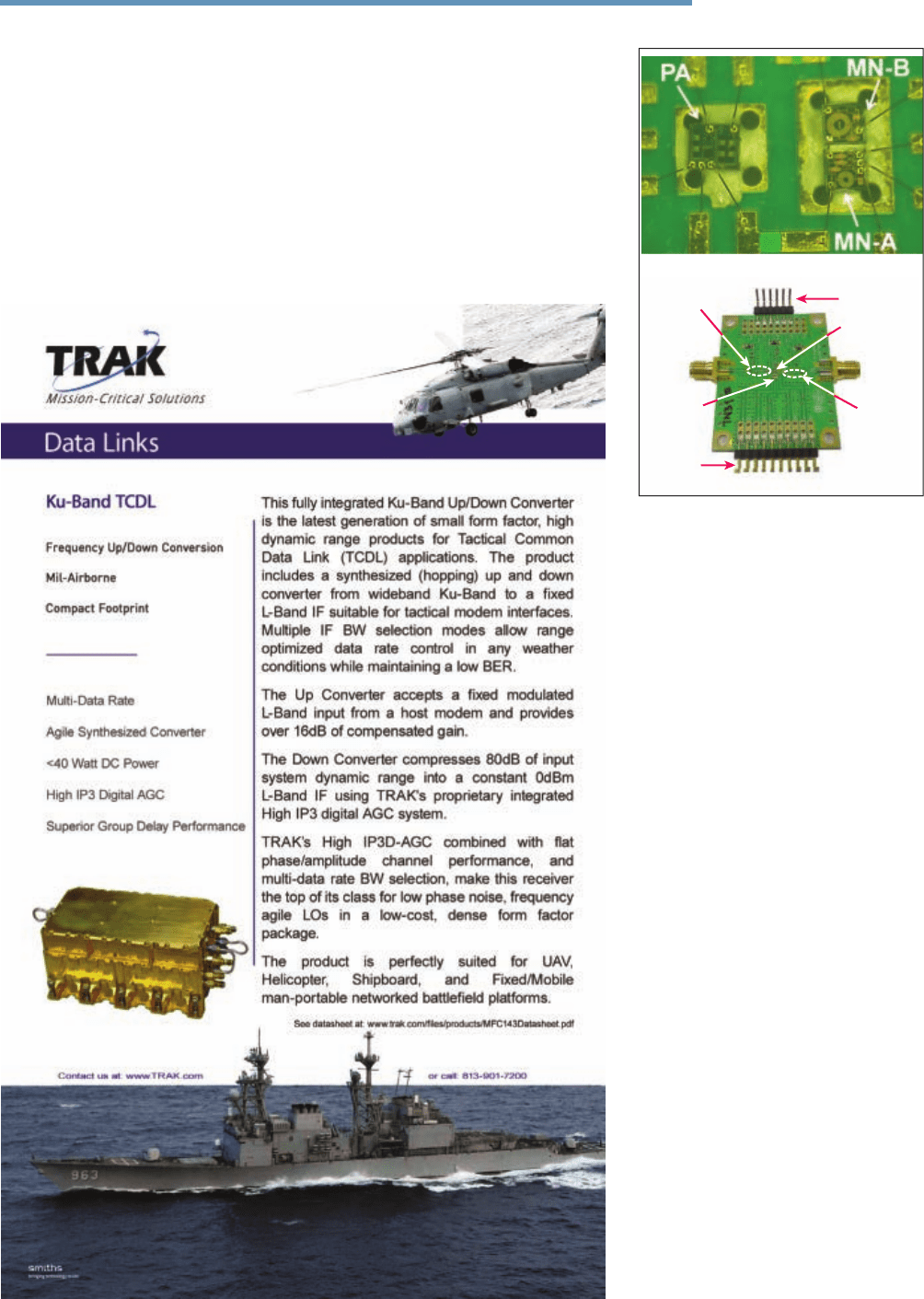
Figure 6 shows the fabricated pro-
totype of the reconfigurable power
amplifier, including the two-stage
power amplifier and the tunable in-
terstage matching network and the
prototype board. The MMIC PA
and MMIC tuner were fabricated on
three different die and co-located on
the prototype board. The die shown
on the left side is a two-stage power
amplifier (PA) having dimensions of
720 m 660 m and the two tuner
die shown on the right side are 600 m
600 m (MN-A and MN-B). These
die are the tunable interstage match-
ing network that provides center fre-
quency tuning function. Separate die
for the tuner were necessary because
of limited wafer space. The input and
output matching networks were fixed
and realized using surface-mount com-
ponents (0402 and 0805 SMT). For the
is shown in Figure 5. This shows the
two-stage amplifier, fixed input and
output matching network, tunable
interstage matching network and the
DC biasing network.
DC Analysis
The circuit is biased using the input
bias V
in
= 1.4 V (I
in
= 1.32 mA), out-
put1 bias V
out1
= 3.6 V (I
out1
= 25.4 mA)
and output2 bias V
out2
= 3.6 V (I
out2
=
137 mA), which are required to oper-
ate the two-stage amplifier. Series RF
chokes and shunt bypass capacitors are
placed between each DC power sup-
ply and the circuit to provide adequate
isolation between each of the amplifier
stages. The center frequency tuning is
performed by changing the control volt-
age of the four FET switches (V
1
, V
2
,
V
3
and V
4
) for turn on or off. Changing
the FET switch state varies the overall
shunt capacitance value (C
2
). To limit
the current flow into each FET switch,
s Fig. 6 Fabricated prototype of the recon-
figurable power amplifier.
MMIC POWER
AMPLIFIER
OUTPUT
MATCHING
NETWORK
(DISCRETE
COMPONENTS)
MMIC
TUNING
ELEMENTS
INPUT MATCHING
NETWORK
(DISCRETE
COMPONENTS)
DC
CONTROL
PINS
DC BIAS PINS
4M32 FINAL.indd 86 3/25/11 3:44 PM
Analog, Digital & Mixed-Signal
ICs, Modules, Subsystems & Instrumentation
2 Elizabeth Drive • Chelmsford, MA 01824
978-250-3343 tel • 978-250-3373 fax • adc@hittite.com
Order On-Line at: www.hittite.com
Receive the latest product releases - click on “My Subscription”
15 New Products Offer Lowest Power Consumption for Best SNR!
IN-STOCK ANALOG-TO-DIGITAL CONVERTERS
Part Number Resolution
Maximum
Sample Rate
# of
Channels
Power
Dissipation
[2][3]
SNR (dBFS) SFDR (dBc) Package
EasySuite™
Evaluation Kit P/N
HMCAD1520 12-Bit 640 MSPS 1, 2, 4 490 mW 70 60 / 75
[1]
LP7D EKIT01-HMCAD1520
HMCAD1511 8-Bit 1 GSPS 1, 2, 4 710 mW 49.8 49 / 64
[1]
LP7D EKIT01-HMCAD1511
HMCAD1510 8-Bit 500 MSPS 1, 2, 4 295 mW 49.8 49 / 65
[1]
LP7D EKIT01-HMCAD1510
HMCAD1102 12-Bit 80 MSPS 8 59 mW / Channel 70.1 77 LP9 EKIT01-HMCAD1102
HMCAD1101 13 / 12-Bit 65 MSPS 8 51 mW / Channel 72.2 82 LP9 EKIT01-HMCAD1101
HMCAD1100 13 / 12-Bit 50 MSPS 8 41 mW / Channel 72.2 82 LP9 EKIT01-HMCAD1100
HMCAD1060 14-Bit 105 MSPS 4 157 mW / Channel 74.3 80 LP7D EKIT01-HMCAD1060
HMCAD1050-80 13 / 12-Bit 80 MSPS 2 102 mW 72 77 LP9 EKIT01-HMCAD1050-80
HMCAD1050-40 13 / 12-Bit 40 MSPS 2 55 mW 72.7 81 LP9 EKIT01-HMCAD1050-40
HMCAD1051-80 13 / 12-Bit 80 MSPS 1 60 mW 72 77 LP6H EKIT01-HMCAD1051-80
HMCAD1051-40 13 / 12-Bit 40 MSPS 1 33 mW 72.7 81 LP6H EKIT01-HMCAD1051-40
HMCAD1040-80 10-Bit 80 MSPS 2 78 mW 61.6 75 LP9 EKIT01-HMCAD1040-80
HMCAD1040-40 10-Bit 40 MSPS 2 43 mW 61.6 81 LP9 EKIT01-HMCAD1040-40
HMCAD1041-80 10-Bit 80 MSPS 1 46 mW 61.6 75 LP6H EKIT01-HMCAD1041-80
HMCAD1041-40 10-Bit 40 MSPS 1 25 mW 61.6 81 LP6H EKIT01-HMCAD1041-40
Hittite Microwave is pleased to announce 15 new Analog-to-Digital Converter (ADC) products that provide ultra low power
dissipation per channel, ease of use and cost efficiency while maintaining high SNR / SFDR performance. When coupled
with Hittite’s RF & microwave IC solutions these new ADCs will optimize your system performance.
160
SAMPLING RATE (MSPS)
RESOLUTION (Bits)
3 20 40 80 105 640 1000
8
10
12/13
14
HMCAD1060
HMCAD1520 - Precision
HMCAD1520 - High Speed
HMCAD1102
HMCAD1510 - High Speed
HMCAD1101
HMCAD1100
65
HMCAD1040-80
500
HMCAD1040-40
HMCAD1041-80
HMCAD1041-40
HMCAD1050-80
HMCAD1050-40
HMCAD1051-80
HMCAD1051-40
HMCAD1511 - High Speed
[1] Excluding Interleaving Spurs. [2] Supply Voltage (Vdd): +1.8 Vdc Analog Supply (AVdd) and +1.8 Vdc Digital Supply (DVdd). [3] Output Supply Voltage (OVdd): +1.7 to +3.6 Vdc.
MWJHITTITE_CONVERTER0411.indd 87 3/25/11 2:15 PM

88 MICROWAVE JOURNAL APRIL 2011
Technical FeaT ure
1 1 0
G H z
V i s i t u s ! 2 0 1 1 M T T S : B o o t h 3 5 1 2
C o n n e c t o r s a n d C a b l e s u p t o
D C t o 2 6 G H z 4 0 G H z t o 1 1 0 G H z
1.0 mm
SMA
N
MMCX
SMPM
High Frequency
Non-Magnetic AVAILBLE!
The three-layer prototype board
has dimensions of 4 cm 5 cm and 50
Ω microstrip lines. The top DC pins
are used to supply the DC bias to op-
erate the two-stage amplifier and the
bottom DC pins are used to switch the
control voltages (V
1
, V
2
, V
3
and V
4
).
imum power transfer is assumed to be
independent of frequency.
low tuning bandwidth (35 percent),
the optimum load impedance for max-
s Fig. 7 Measured and simulated S-pa-
rameters of the GaAs MMIC reconfigurable
power amplifier.
0
–5
–10
–15
–20
–25
–30
–35
4.03.02.01.00
FREQUENCY (GHz)
(a)
(b)
(c)
4.03.02.01.00
FREQUENCY (GHz)
4.03.02.01.00
FREQUENCY (GHz)
m1: f = 1.37 GHz
16.538 dB
m2: f = 1.60 GHz
17.708 dB
m3: f = 1.71 GHz
17.733 dB
m4: f = 1.95 GHz
16.328 dB
m1: f = 1.37 GHz
–26.519 dB
m2: f = 1.60 GHz
–15.662 dB
m3: f = 1.71 GHz
–12.118 dB
m4: f = 1.95 GHz
–8.4243 dB
m1: f = 1.37 GHz
–8.870 dB
m2: f = 1.60 GHz
–10.980 dB
m3: f = 1.71 GHz
–10.176 dB
m4: f = 1.95 GHz
–10.976 dB
S
11
(dB)
0
–5
–10
–15
–20
–25
–30
–35
S
22
(dB)
20
15
10
5
0
S
21
(dB)
m1
m2
m3
m4
m1
m2
m3
m4
m1
m3
m2
m4
TABLE II
BInAry comBInATIons for fET TunIng sTATEs
FET1 FET2 FET3 FET4
Total Shunt
Capacitance
Operating
Frequency
(f
o
)
on on on on 5.86 pF 1.37 GHz
on off off on 2.04 pF 1.60 GHz
on off off off 1.50 pF 1.71 GHz
off off off off 0.09 pF 1.95 GHz
4M32 FINAL.indd 88 3/25/11 3:45 PM
Analog, Digital & Mixed-Signal
ICs, Modules, Subsystems & Instrumentation
2 Elizabeth Drive • Chelmsford, MA 01824
978-250-3343 tel • 978-250-3373 fax • sales@hittite.com
Order On-Line at: www.hittite.com
Receive the latest product releases - click on “My Subscription”
DSP
0
90°
PLL
PLL
÷ N
ADC
ADC
New Dual Baseband Digital VGA & Low Pass Filter Drive Low Power ADCs!
Dual Baseband Low Pass Filter
High Linearity: Output IP3 +30 dBm
Programmable Bandwidth: 3.5 to 50 MHz
Exceptional 3 dB
Bandwidth Accuracy: ±2.5%
6th Order Butterworth
Magnitude & Phase Response
Dual Baseband VGA
High Linearity: Output IP3 +30 dBm
Variable Gain: 0 to 40 dB
High Bandwidth: DC to 100 MHz
Precise Gain Accuracy: 0.5 dB Step
Excellent Magnitude & Phase Match
Ideal for Baseband Signal Processing Before A/D or After D/A Converters for
Point-to-Point Fixed Wireless or Base Station Transceivers!
HMC960LP4E
Dual Baseband
Variable Gain Ampli er
HMC900LP5E
Dual Baseband
Low Pass Filter
New A/D Converter Line Completes Hittite’s Offering from “Antenna-to-Bits”
HMCAD1520
A/D Converter
12-Bit / 320 MSPS
HMC597LP4E
I/Q Demodulator
0.1 - 4.0 GHz
HMC821LP6CE
Tri-Band PLL + VCO
1.72 - 2.08 GHz
HMC822LP6CE
Tri-Band PLL + VCO
665 - 825 MHz
HMC794LP3E
Programmable Divider
÷1, 2, 3, or 4
HMC618LP4E
1.7 - 2.2 GHz LNA
N
EW
!
N
EW
!
MWJHITTITE_BASEBAND0411.indd 89 3/25/11 2:15 PM
90 MICROWAVE JOURNAL APRIL 2011
Technical FeaT ure
www.phasematrix.com
877-447-2736 or 408-428-1000
analysis was used to consider any effects
due to possible variations in the proto-
type board on the circuit performance.
The length and width of the microstrip
lines in the circuit simulations were
varied to ensure that any effects due to
these variations were minimal.
Small-signal Measurement
The small-signal response of the
reconfigurable MMIC PA was sim-
ulated and measured. An Agilent
E5071C Network Analyzer was used
to measure the S-parameters. Table
2 shows the combination of FET
switch tuning states and the total
shunt capacitance value used to tune
the center frequencies to 1.37, 1.60,
1.71 and 1.95 GHz.
Figure 7 shows the measured
(solid lines) and simulated (dotted
lines) S
21
, S
11
and S
22
, at four differ-
ent center frequencies. The fabricat-
ed prototype shows 17 dB (± 0.7 dB)
measured gain and gives reasonable
agreement with the simulated gain.
The measured input reflection coeffi-
cient (S
11
) is less than -10 dB at most
of the operating frequencies. The
output reflection coefficient (S
22
)
varies between -8.5 and -26.5 dB for
the different switch states. The mini-
mum reverse isolation (S
12
) is -50 dB
for all states.
Table 3 shows the measured 3 dB
bandwidth at each operating frequen-
cy and its corresponding Q-factor. The
Q-factor is nearly constant for all tun-
ing states. The measured 3 dB band-
width varied from 260 to 320 MHz
between the tuning states.
Large-signal Measurement
The Agilent MXA N9020A Spec-
trum Analyzer and Agilent MXG
N5181A Analog Signal Generator
were used to measure the large-signal
power performance. OIP3 and P
1dB
for each state were measured at the
corresponding operating frequency
(f
o
) and are tabulated in Table 4. The
maximum measured OIP3 and P
1dB
at
1.370 GHz are 28.25 and 16.62 dBm,
respectively.
of parasitics from the prototype board
were modeled using Sonnet. The
SMT S-parameter data that are avail-
able from the vendors were also includ-
ed in the circuit simulation. A sensitivity
Simulation and
meaSurementS
The circuit simulation was per-
formed using the Agilent Advanced
Design System (ADS) and the effects
taBle iV
meaSured p
1dB
and oip3 for the reconfiguraBle mmic pa
f
o
(GHz) 1.370 1.600 1.710 1.950
Meas P1dB (dBm) 16.62 16.35 14.95 13.85
Meas OIP3 (dBm) 28.25 25.89 24.83 22.61
taBle iii
3 dB Bandwidth at Varying operating frequencieS
f
o
(GHz) 1.370 1.600 1.710 1.950
3 dB BW (MHz) 260 260 270 320
Q= f
o
/BW 5.269 6.154 6.333 6.094
4M32 FINAL.indd 90 3/25/11 3:45 PM