Microwave Journal 2011 №04
Подождите немного. Документ загружается.

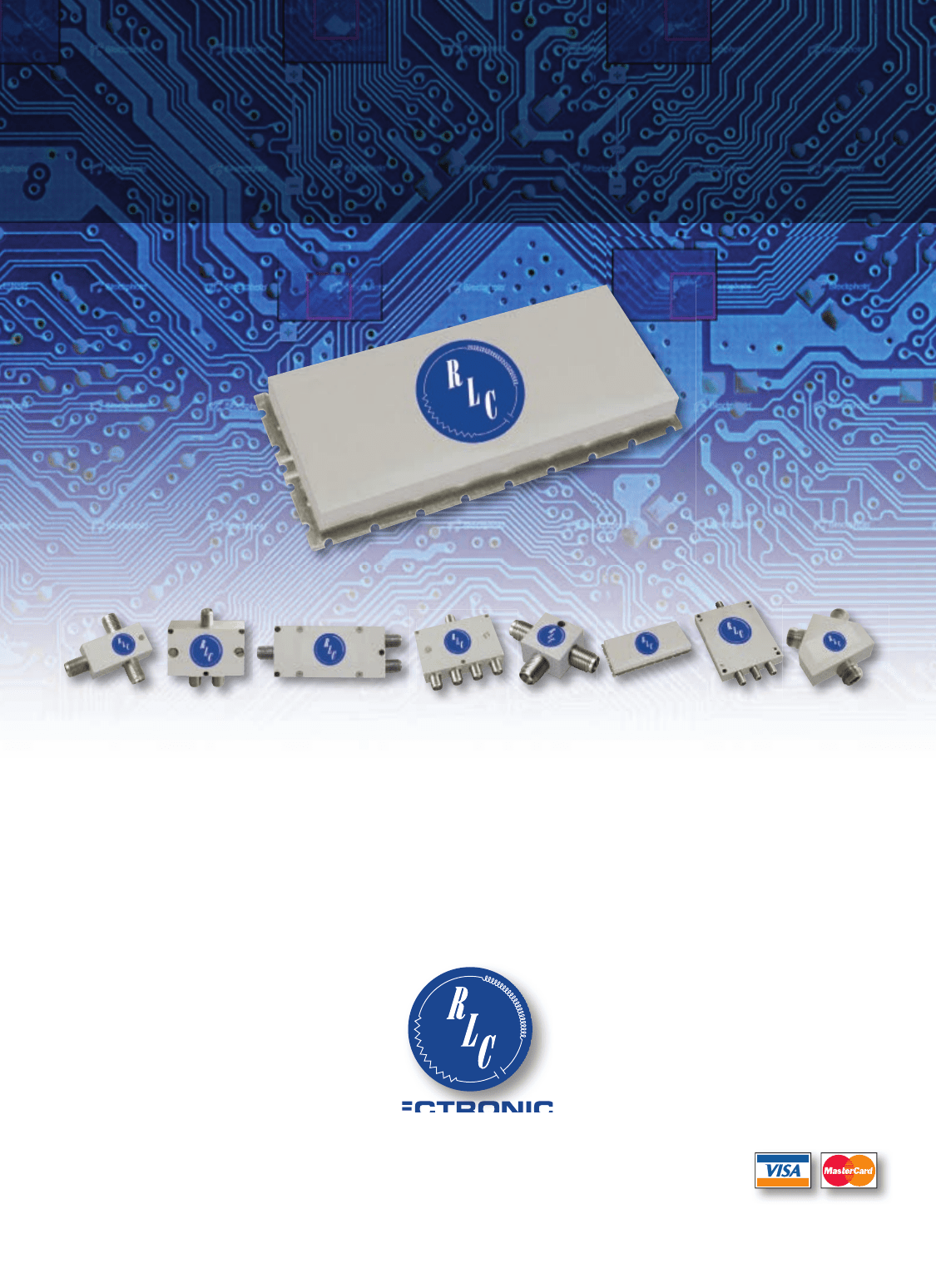
RLC ELECTRONICS, INC.
83 Radio Circle, Mount Kisco, New York 10549 • Tel: 914.241.1334 • Fax: 914.241.1753
E-mail: sales@rlcelectronics.com • www.rlcelectronics.com
ISO 9001:2008 CERTIFIED
■ Our family of Power Dividers are available in a choice
of 2, 3, 4, 6, 8, 9, 12, and 16-way configurations
■ Available in frequencies from DC to 40 GHz
■ A wide choice of connector styles or surface mount
configurations to suit any specific need
■ Proven applications for instrumentation, TelCom,
and SatCom
RLC Electronics’ Power Dividers offer superior
performance in compact microstrip units with wide
bandwidth and multiple outputs. These units provide low
VSWR, high isolation and excellent phase characteristics
between all the output ports.
Since 1959, RLC has been recognized as a leading
designer and manufacturer of high quality, state-of-the-
art components for the microwave & RF industry.
For more detailed information, or to access RLC’s exclusive Filter Selection Software, visit our web site.
RLC is your complete microwave & RF component resource for
Switches, Filters, Power Dividers, Terminations, Attenuators, DC Blocks, Bias Tees & Detectors.
RLC ELECTRONICS, INC.
Model DSM-0520-2
shown here
RLC Power Dividers...
Known for high performance, innovative solutions,
and cost-effective pricing.
RLC29188PwrDivAdMJ.indd 1 3/7/11 2:39 PM
MWJRLC0411.indd 21 3/25/11 1:46 PM
22 MICROWAVE JOURNAL APRIL 2011
COVER FEATURE
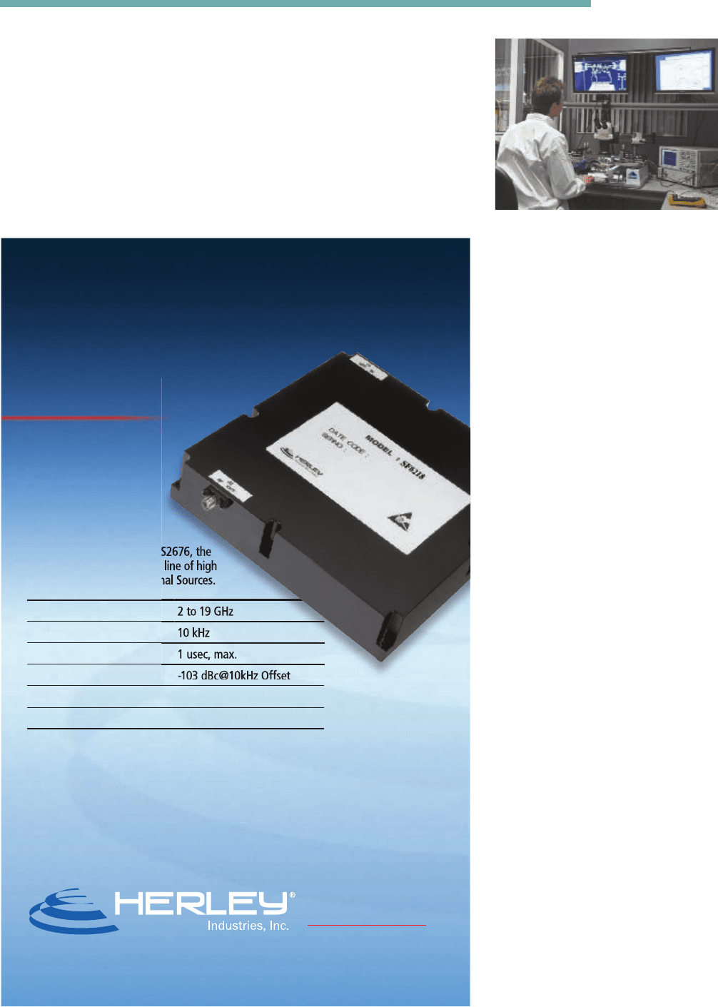
Fast (1 usec)
Indirect
Synthesizer
Herley General Microwave
announces the NEW Model S2676, the
latest addition to its product line of high
performance Microwave Signal Sources.
Wide Frequency Range 2 to 19 GHz
High Resolution 10 kHz
Fast Settling Time 1 usec, max.
Low Phase Noise -103 dBc@10kHz Offset
Low Power Consumption 30 Watts, max.
Small Size 6" x 6" x 1.1"
The Model S2576 is a cost effective solution for today’s
demanding Electronic Warfare, Simulator and Test Systems.
Other Catalog & Custom Microwave Signal
Sources from Herley General Microwave include:
• Digitally Tuned Oscillators (DTO)
• Frequency Locked Oscillators (FLO)
• Voltage Controlled Oscillators (VCO)
Herley New York • 227A Michael Drive, Syosset, NY 11791
Telephone: 516-802-0900 • FAX: 516-802-0897 • E-mail: sales.newyork@herley.com
Proven Microwave
Performance
www.herley.com
Microwave Signal Sources from Herley General Microwave
Your time-trusted
source
Model S2676, the
latest addition to its product line of high
performance Microwave Signal Sources.
2 to 19 GHz
10 kHz
1 usec, max.
-103 dBc@10kHz Offset
source
her2148_SynthAd_HPI_mjD1.indd 1 7/16/10 2:55 PM
ate mm-wave MMICs (shown in Fig-
ure 2) is also very expensive and adds
to the cost of development activity.
While the implementation and evalu-
ation of components targeting the 42
GHz band is less of an issue than for
E-band, the current range of avail-
able components is still limited. This
is starting to change, with suppliers
actively developing MMICs targeting
the 40.5 to 43.5 GHz band, which will
lead to increased component avail-
ability and reduced component cost.
There is also a signifi cant alloca-
tion of mm-wave spectrum at approxi-
mately 60 GHz. The most extensive
and fl exible allocation is in the US,
where the 57 to 64 GHz band is avail-
able for unlicensed use. Two appli-
cations are normally cited for the 60
GHz spectrum: medium range point-
to-point outdoor links and very high
data rate WLANs or wireless personal
area networks (WPAN).
One feature of the 60 GHz spec-
trum is high atmospheric attenua-
tion, caused by oxygen absorption.
This reduces practical propagation
distances, but is often presented as
offering benefi ts in terms of interfer-
ence reduction and ease of frequency
re-use. However, to term the oxygen
absorption an advantage seems like an
attempt to change a vice into a virtue
and the 60 GHz bands look a less at-
tractive option for outdoor point-to-
point links than E-band.
The 60 GHz spectrum, however, is
an attractive option for very high data
rate WLAN/WPAN applications. In
this case, the potential product vol-
umes would be extremely high, the re-
quired performance (NF, linearity and
transmit power) less stringent than for
point-to-point links and the cost tar-
gets very low. These factors lead to the
conclusion that this is an application
that is likely to be dominated by highly
the current range of commercially
available parts is limited and the unit
cost could not be described as low.
The problem is that the development
of E-band MMICs is complex and
time consuming and is therefore very
costly. Unless the MMIC supplier
has confi dence that volume orders
will come through, it can be diffi cult
to justify the NRE costs to develop
E-band components.
The test equipment used to evalu-
licenses to be obtained quickly and
cheaply while retaining the benefi ts of
interference protection.
1
Despite the attractions of E-band,
deployment in very high volumes will
only happen once the price of equip-
ment falls to an acceptable level.
This requires wider availability of
component parts with adequate per-
formance at acceptable costs. While
it is possible to manufacture E-band
MMICs in high volumes at a low cost,
Fig. 2 Evaluation of a mm-wave amplifi er
MMIC in Plextek’s RFOW test laboratory.
4M27 FINAL.indd 22 3/25/11 11:27 AM

CST of America®, Inc. | To request literature (508) 665 4400 | www.cst.com
CHANGING THE STANDARDS
AT THE FRONTIERS OF SIMULATION
CST STUDIO SUITE
2011
Looking for the broader picture? CST STUDIO SUITE 2011 gives you more
than just the details. With a user friendly interface, a choice of first class
solvers, easy data exchange between software tools and world class post-
processing, you can leverage the latest developments in electromagnetic
simulation to bring designs to market faster and with lower risk.
Choose CST STUDIO SUITE 2011 – complete technology for 3D EM.
Explore the
EM simulation universe
MWJCST1210.indd 23 3/25/11 1:46 PM
24 MICROWAVE JOURNAL APRIL 2011
COVER FEATURE
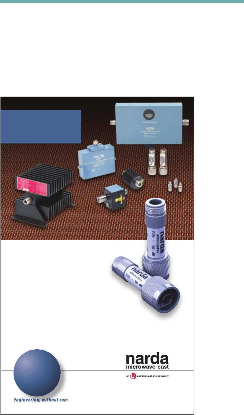
Narda’s Extensive
Family of In-Stock
Attenuators
Narda offers miniature, medium
and high power, fixed, variable
and step configurations. These units
come in an almost limitless combination
of physical and electrical performance
characteristics to meet the needs of
system designers, original equipment
manufacturers, and laboratory users.
■ Frequencies from DC to 40 GHz
■ Values from 0 to 69 db
■ Power Ratings from 0.5 to 150 Watts
Model 779-10
Fixed
Attenuator
435 Moreland Road, Hauppauge, NY 11788
Tel: 631.231.1700 • Fax: 631.231.1711
e-mail: nardaeast@L-3com.com
www.nardamicrowave.com/east
Engineering, without compromise since 1954.
Engineering, without compromise since 1954.
Visit Us
At The
NAB Show
4/9-4/14
Booth
SU8821
NAR29141IsHlfAttnAdMJ.indd 1 2/22/11 11:28 AM
fully released processes can offer use-
ful gain across the required frequency
range. With E-band operation, the
number of potential processes is rel-
atively modest. Transistors realised
on short geometry CMOS and SiGe
processes have a high enough Ft to
provide gain at E-band and numerous
circuits at high mm-wave frequencies
have been demonstrated using these
technologies.
However, all current commercially
available mm-wave links for wireless
backhaul incorporate GaAs-based
front-end MMICs. The reason be-
hind this is that acceptable NF and
adequate linearity are essential re-
quirements and GaAs technology of-
fers superior performance in these
respects.
2
GaN technology shows a
lot of promise for the future,
3
in par-
ticular for the realisation of mm-wave
PAs. However, the GaN foundry pro-
cesses that are commercially available
today are only suitable for operation
to approximately 20 GHz and, for the
immediate future, GaAs technology is
the best candidate for the realisation
of mm-wave amplifi ers for point-to-
point applications.
Other advantages of the GaAs tech-
nology for the realisation of mm-wave
amplifi ers include the semi-insulating
substrate material and the ready avail-
ability of low inductance through sub-
strate vias. The absence of these fea-
tures on most Si processes means that
the design approaches that must be
adopted tend to sacrifi ce gain. Avail-
able gain decreases with increasing
operating frequency and at E-band
the available gain of transistors on
commercially available processes is
very limited. In the 42 GHz band, the
available gain is much higher, which
eases the design process and increases
the linearity and output power that
can be achieved. However, the same
range of candidate processes can be
considered for both frequency ranges.
The commercially available GaAs
processes that can provide useful gain
up to E-band can be split into three
categories:
• 0.15 or 0.13 µm gate length
PHEMT
• 0.15 µm gate length MHEMT
• 0.1 µm gate length PHEMT
There is a minimum level of avail-
able transistor gain below which it is
not practical to consider realising am-
for operation above 40 GHz, using
commercially available foundry pro-
cesses and offers some guidelines for
achieving optimum performance and
reduced risk.
PROCESS AVAILABILITY AND
SELECTION
The fi rst consideration when
choosing a process for the realisation
of mm-wave amplifi er ICs is to iden-
tify which commercially available,
integrated Si transceivers.
There may be a role for small,
low-cost transmit amplifi er MMICs
capable of modest output power lev-
els. However, increased confi dence
in high production volumes is needed
before the work required to drive
down the size and cost to the levels
required for WLAN/WPAN applica-
tions will be undertaken.
This article considers the chal-
lenges in designing amplifi er MMICs
4M27 FINAL.indd 24 3/25/11 11:28 AM

MWJANSYS0211.indd 25 3/25/11 1:47 PM

26 MICROWAVE JOURNAL n APRIL 2011
Cover Feature
or 0.13 µm gate length PHEMT pro-
cesses can provide a good level of gain
across the 42 GHz band. However, at
E-band, the maximum practical tran-
sistor size that can be used in these
processes (in order to retain an ac-
ceptable level of available gain) is rela-
tively small. Larger device sizes can be
considered with a 0.1 µm gate length
process, which means that the achiev-
able linearity and output power levels
are higher. Bias conditions and break-
down voltage must also be assessed
when comparing the linearity avail-
able from different processes, but,
even with this consideration in mind,
it is possible to say that of today’s com-
mercially available GaAs processes,
the best choice for output power and
linearity at E-band is the 0.1 µm gate
length PHEMT.
Obviously process costs also need
to be considered. GaAs processes
with 0.1 µm geometries tend to utilise
e-beam written gates, which can push
up process costs. Some 0.13 and 0.15
µm processes have optically defined
gates, which should result in lower
production costs. This difference is
likely to change over time and it is ex-
pected that GaAs processes with op-
tically defined gates at lengths of 0.1
µm and below will become commer-
cially available in due course.
The available substrate height
(thickness) also needs to be consid-
ered when selecting the preferred
process. Most commercially avail-
able GaAs processes have a substrate
thickness of 100 µm. However, some
processes are available with a thinner
substrate thickness of 50 µm, which
can provide a performance advan-
tage at mm-wave frequencies. The
advantage stems from the reduced
via inductance inherent in the thinner
substrate. The via inductance acts as
series inductive feedback around the
transistor and can degrade perfor-
mance and stability.
This is apparent by inspection of
the simulated maximum available gain
(MAG) versus frequency curves found
in Figure 3.
4
These curves are for a
0.15 µm gate length process with a
100 µm substrate height. At low fre-
quencies, the device is conditionally
stable (or potentially unstable with
K<1) and the gain response plotted
is actually the maximum stable gain
(MSG). The kink in the traces, at ap-
wider unit gate width), the parasitic
effects increase (that is gate induc-
tance and phase delay between gate
fingers). This reduces the available
high frequency gain of the transistors.
For a given process and bias point,
there is thus a maximum transistor
size that can be considered for a par-
ticular frequency range, which limits
the maximum RF power handling and
linearity of the transistor.
Most commercially available 0.15
plifier blocks. In the authors’ experi-
ence, 6 dB is a realistic lower limit.
The available gain of a transistor is
not only dependent on the process, it
is also dependent on device geometry
(number of gate fingers and unit gate
width), substrate thickness (actually
parasitic inductance of through sub-
strate vias used as RF grounding) and
the bias point.
As the total transistor gate width
increases (more gate fingers and/or
4M27 FINAL.indd 26 3/29/11 9:47 AM

3
Model
Noise
Figure
Gain
Output
P1dB
Gain
Flatness
VSWR
In / Out
Price
Start Stop (dB) Max. (dB) Min. (dBm) Min. (± dB) Max.
Domestic, U.S.
BZP540A 0.5 40 5.5 25 8 2.5 2.5:1 $985
BZ2640A 26 40 4.5 25 8 2.0 2.5:1 $985
BZ1826A 18 26 2.5 28 8 1.0 2.0:1 $875
BZP518A 0.5 18 2.7 30 10 1.8 2.5:1 $985
BZ0618B 6 18 1.8 30 10 1.5 2.0:1 $985
BZ0412B 4 12 1.6 28 10 1.5 2.0:1 $785
BZP506A 0.5 6 1.4 25 10 1.3 2.0:1 $875
BZP504F 0.5 4 1.3 30 17 1.0 2.0:1 $985
BZ0204F 2 4 1.0 30 17 0.5 2.0:1 $685
BZ0102F 1 2 1.0 30 17 0.5 2.0:1 $685
Frequency
Range (GHz)
TECHNOLOGIES
INNOVATING TO EXCEL
Ph: +1 (631) 444-8827
Fax: +1 (631) 444-8825
E-Mail: info@bnztech.com
Web: www.bnztech.com
Made in USA
AMPLIFIERS
FROM
STOCK!
Ultra High Performance!
Ultra-Wide Bandwidths!
Models to 40 Ghz!
3 Year Warranty!
Operating Temperature:
Reverse Polarity Protected
Internal Voltage Regulator
Smallest Housing
RoHS Compliant
Drop-In ?
Just Remove Connectors!
-
55° to +85° C
Delivery from stock to 7 days!
For the full list Visit www.bnztech.com/fastamps
Contact us for a quote with YOUR custom specifications.
MWJB&Z0411.indd 27 3/25/11 1:48 PM

28 MICROWAVE JOURNAL n APRIL 2011
Cover Feature
(through substrate vias directly under
the fingers of the transistors) can also
help reduce source grounding induc-
tance.
Design, simulation anD
example mmiCs
Once the process has been select-
ed, detailed investigations into the
design can commence. At E-band fre-
quencies, the first challenge is achiev-
ing adequate gain as the transistors
have little in hand to be sacrificed.
At each stage of the design process,
care must be taken to ensure as little
gain as possible is lost, with practical
implementation issues such as bias-
ing the device and realising a practical
matching network.
4
Obviously, stability must also be
considered. The transistors have a lot
of low frequency gain and care must
be taken to ensure the design is stable
in this region. If transistors are used
that revert to a region of potential in-
stability at higher frequencies, care
must also be taken in this region. In
both cases, any components added to
ensure stability must not add any sig-
nificant in-band loss.
The other challenge with gain is
linked to linearity. Larger transistors
at higher bias currents must be used,
if increased power handling and/or
linearity is required. These larger
transistors have reduced gain and for a
given process and operating frequen-
cy range there will be a maximum
transistor size that can be considered
if practical levels of gain per stage are
to be achieved.
This effect will be evident at both
40.5 to 43.5 GHz and at E-band, but
the use of larger transistors will be
more practical in the 42 GHz band and
higher power/linearity amplifiers can be
tained from the device would not be
adequate.
This occurs because the reverse
isolation is reducing with increasing
frequency (feedback is increasing),
but the transistors still have significant
forward gain. If the source inductance
of the transistors can be reduced, this
reversion to potential instability can
be suppressed. The use of a thinner
substrate height can allow this. The
availability of intersource grounding
proximately 40 GHz, marks the point
at which the transistor transitions to
being unconditionally stable (K>1).
This behaviour is well understood.
The more curious aspect to the
curves is the second higher frequency
kink, which shows the transistors re-
verting to a region of potential insta-
bility. If operated in this region, some
gain must be sacrificed to stabilise
the transistor and it is likely that the
practical performance that can be ob-
s Fig. 3 MAG/MSG for 0.15 µm PHEMT
process, 50 µm finger width and varying num-
ber of fingers on a 100 µm thick substrate.
20
15
10
5
0
100806040200
G
max
(
dB
)
FREQUENCY (GHz)
num_fngrs = 8 num_fngrs = 6
num_fngrs = 4 num_fngrs = 2
4M27 FINAL.indd 28 3/25/11 11:28 AM
®
The Design Engineers Search Engine finds the model you need, Instantly • For detailed performance specs & shopping online see
IF/RF MICROWAVE COMPONENTS
ISO 9001 ISO 14001 AS 9100 CERTIFIED
P.O. Box 350166, Brooklyn, New York 11235-0003 (718) 934-4500 Fax (718) 332-4661
®
U.S. patent 7739260
478 rev D
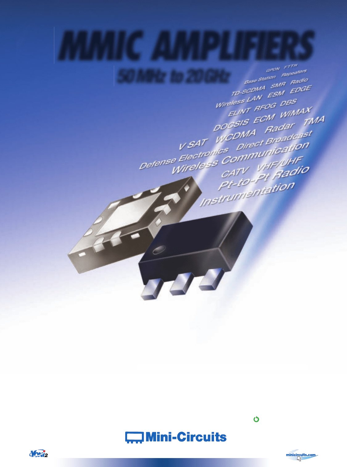
MMIC AMPLIFIERS
50 MHz to 20 GHz
WOW!
COVER 50 MHz to 20GHz WITH ONLY 2 AMPLIFIERS !
A wide operating bandwidth can mean a tradeoff in performance. Not with these amplifiers. With just two
Mini-Circuits MMICs, you can cover the entire spectrum from 50 MHz to 20 GHz, with outstanding electrical
performance — making them an exceptional value for their price.
The PHA-1+ is a highly advanced E-pHEMPT amplifier poised to be a workhorse for your wireless applications.
Why? It offers ultra-high dynamic range but with low noise, and has among the highest IP3 performance
(42 dBm typical at 2 GHz) of any amplifier in its class. The PHA-1+ has good input and output return
losses over an extremely broad frequency range (50 MHz to 6 GHz) and can work without external matching
components - saving you cost, design time and board space. The PHA-1+ is ideal for use in LTE and
TD-SCDMA systems. ACLR and EVM data is available on our website.
The AVA-24+ can cover 5 to 20 GHz with excellent gain flatness (+/- 0.8 dB) across its entire frequency range,
with integrated matching circuits and bias circuit in an easy-to-use surface-mount package. Its high isolation
(37dB typical) makes it very useful as a buffer amplifier. This design approach makes the AVA-24+ an extremely
flexible MMIC that is simple and straightforward to use.
Full electrical, mechanical and environmental specifications for both of these models, as well as characterization
data including S-parameters and performance curves, are available at minicircuits.com. These models are in
stock for immediate shipment.
AVA-24+
$
19.95
ea. ( Qty. 1-9)
PHA-1+
$
1.49
ea. ( Qty. 50)
RoHS compliant
Mini-Circuits…we’re redefining what VALUE is all about!
478 rev D.indd 1 11/23/10 12:05:42 PM
MWJMC_478REVD_0411indd 29 3/25/11 1:56 PM
30 MICROWAVE JOURNAL n APRIL 2011
Cover Feature
simulated performance.
4
This was
fabricated on the PP15-20, 0.15 µm
gate length PHEMT process of WIN
Semiconductor. This process has a
100 µm thick substrate and is prob-
ably not the ideal choice for E-band
MMICs, but it demonstrates over 4
dB of gain per stage in the 71 to 76
GHz band and, perhaps more impor-
tantly, shows a reasonably good match
between simulated and measured
performance. In addition to accurate
EM simulation, this requires good de-
vice models, which are valid across the
frequency range of interest.
Figure 5 shows a Plextek designed
1 W, 40.5 to 43.5 GHz PA, designed
for a 0.15 µm gate length PHEMT
process. The approach taken for this
design was to identify the transistor
geometry and bias capable of offer-
realised. Obviously, linearity and power
handling can be increased by RF power
combining of multiple transistors, but
the losses of the combining structures
make this a process of diminishing re-
turns. However, it is still the most ap-
propriate route to designing high pow-
er/linearity mm-wave amplifiers.
The PHEMT processes that are
best suited to mm-wave operation
generally have very good NF perfor-
mance. The NF exhibited by a given
transistor is set by the impedance pre-
sented to the transistor and the losses
at its input (that is the input matching
network losses). The impedance re-
quired to achieve best NF is different
from that required to achieve good
input return loss and so optimise the
gain of the device. One approach to
achieving improved NF is to simply
match for optimum noise and live with
the degraded input match (and re-
duced gain). Other approaches aimed
at simultaneously achieving good in-
put return loss and NF performance
include adding series inductive feed-
back or adopting a balanced design.
Unfortunately, these techniques all
require some loss of gain and while
they can be considered for 40.5 to 43.5
GHz operation, they are not practical
at E-band using current commercially
available processes. The only practi-
cal approach is to select a device size
and bias point with a lowest NF in
mind and then to conjugately match
for maximum gain and to accept the
resulting performance.
It is normal to start the amplifier
design process with ideal passive ele-
ments and active device models. Once
acceptable performance is achieved,
the design is moved to a practical
implementation with the incorpora-
tion of representative passive models,
including those required to simulate
parasitics and discontinuities. With
mm-wave circuits, it is always essen-
tial to perform an EM simulation to
accurately account for all proximity
and discontinuity effects associated
with the layout. Many 3D and 2.5D
EM simulation packages are now
available. In the authors’ experience,
the use of a 3D simulator for simula-
tion of a MMIC does not guarantee
superior performance to that using a
2.5D simulator.
Figure 4 is a photograph of an
E-band gain block, together with a
comparison of the measured and EM
s Fig. 4 E-band gain block realized with a
0.15 µm PHEMT process: (a) photograph and
(b) measured and simulated performance.
10
5
0
–5
–10
–15
–20
–25
1009080706050
FREQUENCY (GHz)
(a)
(b)
S
11
and S
21
MEASURED (dB)
S
11
and S
21
SIMULATED (dB)
s Fig. 5 Plextek designed 1 W, 40.5 to
43.5 GHz power amplifier.
The First Name in
M
icrowave
Delivering GaAs
pHEMT switches
with a gate lag
time of less than
20 nanoseconds
macomtech.com
Switches available from
10 MHz to 20 GHz
MWJ_Apr2011_MACOMTech_third strip.qxd:Layout
4M27 FINAL.indd 30 3/25/11 11:29 AM