Marulanda J.M. (ed.) Electronic Properties of Carbon Nanotubes
Подождите немного. Документ загружается.


Low-Energy Irradiation Damage in Single-Wall Carbon Nanotubes
345
observed the conversion of the electric properties at 28 K (Vijayaraghavan et al., 2005). Further
irradiation caused an increase of the nominal band gap observed in the low-temperature
electric properties. More recently, we succeeded in converting the room-temperature device
characteristics from metallic to semiconducting by local irradiation using an electron beam
lithography system (Suzuki et al., 2008). Before the irradiation, the device characteristics were
almost gate-independent, which is a common feature of a metallic SWCNT. A part of a
metallic SWCNT was once scanned by an electron beam. Then, the room-temperature gate
characteristics of the device were converted to semiconducting, as shown in Fig. 12(a). After
the irradiation, ambipolar semiconducting gate characteristics were clearly observed.
Room-temperature Coulomb oscillations have been observed when defects form a small dot
in a SWCNT channel (Matsumoto et al., 2003). The low-energy irradiation damage can also
be used to fabricate such small dots intentionally. As shown in Fig. 12(b), after irradiation,
multi-dot Coulomb oscillation properties are sometimes observed at room temperature.
A schematic model of a possible mechanism for the irradiation-induced semiconducting
properties is shown in Fig. 12(c) (Kanzaki et al., 2007. Suzuki et al., 2008). The temperature
dependence of device characteristics after irradiation shows that an energy barrier for
carriers is formed in the SWCNT channel. The barrier height observed in the electric
properties reaches about 0.6 eV, when irradiation-induced semiconducting properties are
observed at room temperature. Recently, a STM study more directly showed that a local
band gap is actually formed in a metallic SWCNT by a carrier injection-induced defect
(Yamada et al., 2009). This suggests that the defect-induced local band gap opening is the
origin of the barrier. The carrier transport is inhibited by the barrier at the gate voltage of
around 0 V. The device still turns on at large gate voltage. This can be reasonably explained
in terms of gate-induced band bending in a metallic SWCNT. The density of states near the
Fermi level of a metallic SWCNT is very small. Owing to the small density of states near the
Fermi level, we can bend the band by applying gate voltage and reduce the effective barrier
height for an electron. At sufficiently large gate voltage, the device will turn on. Thus, the
metal-semiconductor transition is explained by the defect-induced barrier formation and
gate-induced band bending. When Coulomb oscillation is observed, the defects seem to act
as tunneling barriers, as schematically shown in Fig. 12(d). In this case, tiny multi-dots
divided by the defects seem to be formed in the vicinity of the irradiated part.
The defect-induced conversion of the electric properties seems to be caused by defects
formed by other methods. In fact, conversion of the electric properties from metallic to
semiconducting also occurs when defects are induced by plasma treatment of metallic
SWCNT-FETs. More interestingly, the defect-induced semiconducting electric properties
well explain the fact that the ratio of “semiconducting” SWCNTs that act as FETs has been
reported to strongly depend on the growth method (Suzuki et al., 2008, Mizutani et al.,
2009). The plasma-enhanced CVD method has been reported to produce preferentially
semiconducting SWCNTs, and the ratio of semiconducting SWCNTs has been reported to
reach about 90 % (Li et al., 2004. Ohnaka et al., 2006) or even 97 % (Mizutani et al., 2009). On
the other hand, for the laser ablation method, which generally produces high-quality
SWCNTs, the semiconducting SWCNT ratio was evaluated to be quite small, about 30 % (Li
et al., 2004). I think that the growth method dependence of the ‘‘semiconducting’’ SWCNT
ratio is mainly due to the growth method dependence of defect density. Distinguishing
whether the electronic structure is metallic or semiconducting by electric measurements
may be inconclusive, especially when the SWCNT shows “semiconducting” properties.

Electronic Properties of Carbon Nanotubes
346
6. Mechanism of the low-energy irradiation damage
The low-energy irradiation damage can be caused by 10-eV photons, which have very small
momentum. This indicates that the momentum of an incident particle would have no
essential role in the damage, which is in remarkable contrast to knock-on damage. Thus, the
defect formation would be due to bond breaking, which follows an electronic excitation by
the energy of the incident particle. An energy of 10 eV is still high enough to cut C-C
bonds. Thus, it is reasonable that low-energy irradiation creates a defect with finite
probability if the defect structure is stable and the lifetime is long enough. A simple example
of this kind of structural change is photodissociation of a molecule. A bond breaking
following electronic excitation can easily dissociate a small molecule In a bulk crystal, on the
other hand, even the breaking of several bonds would result in immediate re-bonding
without any structural change because an atom has very little freedom of displacement due
to the existence of surrounding atoms. The situation in a SWCNT is one between a molecule
and bulk. More than one bond breaking would be necessary to stabilize the defect. Among
related carbon materials, low-energy electron and photon irradiation-induced structural
change (polymerization) is known to occur for fullerenes. On the other hand, the damage
has not been reported for graphite or MWCNTs, as discussed in sec. 4.7.
Interestingly, Yamada et al. (Yamada et al., 2009) have proposed, on the basis of thier STM
results, that carrier injection first creates primary defects whose lifetime is very short (<50
ms). Most of them are quickly annihilated and the structure is restored. However, in rare
cases, a primary defect fails to recover and a stable defect is created. The quantum efficiency
of the primary defect formation was evaluated to be 2×10
-10
at a bias voltage of 3.5 V near
the defect creation threshold.
The detailed atomic structure of a low-energy irradiation-induced defect is not clear at
present. A detectable change has not been observed even with microscopy techniques, such
as SEM. This is one of the main reasons that the low-energy irradiation had not been
recognized for such a long time, although SEM had been commonly used for characterizing
SWCNTs since their discovery. Our previous TEM observation showed that the tube wall is
not clearly destroyed regardless of severe damage (Suzuki et al., 2005b). The Stone-Wales
defect, which is formed by a C-C bond rotation, is consistent with the conservation of the
number of carbon atoms. However, the stable structure seems to contradict the relatively
small activation energy and healing at a moderate temperature or even at room temperature
or below. Another possible defect is a vacancy in the tube wall with a migratory C adatom
on the surface. The observed activation energies (0.7-1.4 eV, sec. 4.5) are very close to the C
adatom migration energies, which are theoretically predicted to depend on the SWCNT
diameter and to be 0.6 to 1.3 eV (Krasheninnikov et al., 2004). However, a high-resolution
TEM observation has shown that annihilation of the vacancy and migratory adatom is
governed by the recombination barrier rather than by the adatom migration barrier itself
(Hashimoto et al., 2004). The existence of such a vacancy-adatom defect (with the adatom
bounded in the vicinity of the vacancy) was also strongly suggested by a scanning tunneling
microscopy study (Lee et al., 2005). The vacancy-adatom defect is simply formed by
breaking two bonds of a C atom. The recombination barrier of the vacancy-adatom defect in
SWCNTs has been calculated to be 1-2 eV (Okada, 2007), which is rather close to the
observed activation energies. Determining the presice defect structure is a future issue.

Low-Energy Irradiation Damage in Single-Wall Carbon Nanotubes
347
7. Other types of damage and irradiation-induced phenomena
The low-energy irradiation damage is often confused with other types of damage and
irradiation-induced phenomena. Here, I would like to summarize differences in the defect
characteristics of low-energy irradiation damage and other damages.
7.1 Knock-on damage
Knock-on damage is caused by ballistic ejection of an atom from a solid by an incident
particle. Thus, the damage is accompanied by a loss of SWCNT mass. The displacement
energy (kinetic energy at which an atom can escape from the solid.) in a SWCNT is
considered to depend on the diameter and to be 15-20 eV. However, when the incident
particle is an electron whose mass is much smaller than a carbon atom, the threshold energy
becomes 80 keV from the energy and momentum conservation laws. The threshold energy
for a photon will be much larger. Thus, the energy at which knock-on damage is observed is
much larger than that at which the low-energy irradiation damage is normally observed.
Knock-on damage occurs in MWCNTs and graphite. For a recent review focusing on carbon
and other nanomaterials, see (Krasheninnikov, 2010).
7.2 Contaminant effects
Low-energy irradiation often causes hydrocarbon contaminants to adhere to the sample
surface. The contaminant adhesion is prominent in a conventional SEM, in which a UHV is
usually unavailable. At the electron energy where severe damage is observed (1 keV or
smaller), severe contaminant adhesion is also observed. This is because the interaction both
between electrons and a SWCNT and between electron and hydrocarbon gases are strong at
such a low energy. However, effects caused by the damage and by the contaminant
adhesion can be easily distinguished by annealing. The contaminants do not sublimate even
at 900 C, whereas the low-energy irradiation damage can be recovered by annealing at
moderate temperatures, as discussed in sec. 4. In our experiments, it is rather difficult to
detect contaminant effects because the spectra or electric properties of pristine SWCNTs and
SWCNTs recovered from the damage are almost identical (see Figs. 6 and 7), although I do
not deny that the contaminants cause some so-called environmental effects (Ohno, 2010).
7.3 Damage by radicals
Irradiation in remnant gases can also cause radical-induced etching, which is the opposite of
the contaminant adhesion. For example, the cutting of MWCNTs has been clearly
demonstrated under gas atmosphere formed by intentional gas bleeding (Yuzvinsky et al.,
2005). In this way, the damage by radicals is generally accompanied by etching, which
eventually cuts and eliminates CNTs. Thus, this damage can not be fully recovered. In some
literatures, reversible chemisorption and desorption on SWCNT or graphene has been
suggested. However, spectra before chemisorption and after desorption by annealing are
often compared after arbitrary normalization. This damage also occurs in thick MWCNTs
and graphite, although some diameter dependence of the damage is observed (Yang et al.,
2006, Zhang et al., 2006b). Metallic SWCNTs are preferentially damaged by radicals (Yang et
al., 2006. Zhang et al., 2006b), although such preference has not been observed for low-
energy irradiation damage. Moreover, severer damage is observed at higher temperatures
due to more activated chemical reactions (An et al., 2002. Zhang, 2006a). This is entirely
opposite to the low-energy irradiation damage (sec. 4.4). Of course, the radical effect

Electronic Properties of Carbon Nanotubes
348
becomes severer at higher pressures and negligible in a UHV. Reader should recall that low-
energy irradiation damage occurs in a UHV after thorough degassing, although no
indication of chemical reaction is observed (sec. 4.6).
In a standard SEM in which the adhesion of contaminants occurs, the radical effects seem to
be less important. Otherwise, the contaminants would not adhere due to etching. According
to my experience, intensive irradiation in a conventional SEM can not cut or eliminate even
a SWCNT (Fig. 7). I suppose that the radical effects are largely suppressed due to the
adhesion of contaminants, which would protect the sample surface (sec. 3.2).
7.4 Substrate charging effects
There has been an attempt to explain the electric property changes by irradiation-induced
charging of the substrate (back-gate dielectric) just under the SWCNT (Marquardt et al.,
2008. Vijayaraghavan et al., 2010). They observed a large conductivity decrease of on-
substrate SWCNT devices by electron irradiation in a SEM. Furthermore, they reversibly
and repeatedly recovered the electric properties by applying a high bias voltage (10 V) to
the SWCNT. The phenomena they observed seem to be essentially the same as ours.
However, they ascribed the conductivity decrease to a local band gap opening caused by
irradiation-induced charging of the dielectric SiO
2
layer just under the SWCNT. Actually,
theoretical calculations predict that a uniform (Li et al., 2003) or inhomogeneous (Rotkin &
Hess, 2004) electric field can open a gap in a metallic SWCNT of specific chiralities.
Marquardt et al. (Marquardt et al., 2008) and Vijayaraghavan et al. (Vijayaraghavan et al.,
2010) think that electron irradiation in a SEM causes such local and inhomogeneous
charging of the dielectric. In their model, the recovery is explained by a release of trapped
charges in the vicinity of the SWCNT caused by the high-bias voltage applied to the drain
electrodes. In a conventional on-substrate device, a large electric field may be produced by
irradiation-induced charging, considering that the field strength is inversely proportional to
the square of the distance.
However, the substrate charging model does not at all explain the fact that the irradiation-
induced conductivity decrease is as ever observed for suspended SWCNTs, as shown in Fig.
4. The theoretical calculations have predicted that an extraoridinarily high electric field of 1
Vnm
-1
barely opens a band gap of several ten milli-electron volts. It is very unlikely that
such a high electric field is formed at SWCNTs suspended 300 nm above the substrate. In
fact, a simulation has been performed under a condition where the gate voltage was applied
from a metal tip located only 0.5 nm from a SWCNT (Rotkin & Hess, 2004). Similarly, this
model cannot explain the degradation of Raman and PL spectra of suspended SWCNTs
(Figs. 1 and 9). Moreover, electron (hole) injection-induced band gap opening has been
observed for a metallic SWCNT lying on a metal substrate, which does not have charge trap
sites (Yamada et al., 2009). This model does not explain the observed band gap value, either.
The calculations show that the maximum value of the field-induced band gap is at most 0.1
eV, which is not sufficient to explain the almost insulating properties observed at room
temperature. In fact, an energy barrier of 0.6 eV was observed for a SWCNT whose room-
temperature electric properties were converted from metallic to semiconducting by
irradiation (sec. 5). Finally, it should be noted that the irradiation-induced conductivity
decrease has been observed in all measured SWCNTs, whereas, in the theoretical
calculations, band gaps open only in SWCNTs having certain chiralities. Considering that
the irradiation-induced physical property changes can recover at a moderate temperature
(300 C [Fig. 7]), the high bias-induced recovery observed in refs. 7 and 8 seems to be due

Low-Energy Irradiation Damage in Single-Wall Carbon Nanotubes
349
to annealing by Joule heating. I do not deny an electric field-induced band gap opening in a
metallic SWNT. However, I do not think that such a high or inhomogeneous electric field is
produced by simple SEM observation or line scans.
7.5 Irradiation-induced heating effects
Low-energy electron and photon irradiation may increase the temperature of the irradiated
SWCNTs. However, the heating effect itself does not explain the low-energy irradiation
damage at all because less damage is observed at higher temperatures, as shown in Fig. 1.
Originally, SWCNTs are thermally very stable materials. Thus, at least under usual
conditions, irradiation-induced heating itself would not damage the SWCNTs in a vacuum,
if ever. In practice, damage is often observed during Raman measurements in air when the
excitation laser power is too large. However, this is not low-energy irradiation damage, but
instead would be combustion, because this damage is not observed in a vacuum or an inert
gas atmosphere.
8. Conclusion
I have shown that low-energy electron and photon irradiation solely damages SWCNTs. The
low-energy irradiation damage extinguishes the characteristic optical and electric properties
and reduces chemical tolerance. Thus, we have to pay attention to the damage when we use
analytical tools that use low-energy electrons (SEM, LEEM etc.) and VUV light or soft X-rays
(photoemission spectroscopy using bright light). The defects have some unique properties.
The damage and recovery are reversible, indicating that the number of carbon atoms is
preserved. The damage strongly depends on diameter. That is, thinner SWCNTs are more
severely damaged. The damage has been observed in SWCNTs but not in MWCNTs,
suggesting that it is characteristic of low-dimensional structures or nanostructures. The
activation energy of the defect healing depends on the extent of the damage and was
evaluated to be about 0.7 to 1.4 eV. Because of the relatively small activation energy, the
defects can be healed even at room temperature or below, and less damage occurs at higher
temperatures. I also showed that the irradiation-induced defects can convert the room
temperature electric properties of a metallic SWCNT to semiconducting. The conversion can
be explained by the local band gap opening caused by the defect and gate-voltage-induced
band bending in the metallic SWCNT. Energetically, the low-energy is still sufficiently
larger than the C-C bond energy and can therefore break the bonds. Future studies should
address the detailed defect structure.
9. Acknowledgment
This work has been done through cooperation of many coworkers. I thank all of my
coworkers for their cooperation and assistance in this work.
10. References
An, K. H.; Heo, J. G.; Jeon, K. G.; Bae, D. J.; Jo, C.; Yang, C. W.; Park, C. Y.; Lee, Y. H.; Lee, Y.
S. & Chung Y. S. (2002). X-ray photoemission spectroscopy study of fluorinated
single-walled carbon nanotubes. Appl. Phys. Lett. Vol. 80, No. 22 (April 2002), pp.
4235-7.

Electronic Properties of Carbon Nanotubes
350
Arima, S.; Lee, S.; Mera, Y.; Ogura, S.; Fukutani, K.; Sato, S.; Tohji, J. & Maeda, K. (2009).
Electron-stimulated defect formation in single-walled carbon nanotubes studied by
hydrogen thermal desorption spectroscopy. Appl. Surf. Sci. Vol. 256, No. 4 (June
2009), pp. 1196-9.
Bachtold, A.; Henny, M.; Terrier, C.; Strunk, C.; Schonenberger, C.; Salvetat, J. P.; Bonard, J.
M. & Forro, L. (1998). Contacting carbon nanotubes selectively with low-ohmic
contacts for four-probe electric measurements. Appl. Phys. Lett. Vol. 73, No. 2 (July
1998), pp. 274-6.
Berthe, M.; Yoshida, S.; Ebine, Y.; Kanazawa, K.; Okada, A.; Taninaka, A.; Takeuchi, O.;
Fukui, N.; Shinohara, H.; Suzuki, S.; Sumitomo, K.; Kobayashi, Y.; Grandidier, B.;
Stievenard, D. & Shigekawa, H. (2007). Reversible defect engineering of single-
walled carbon nanotubes using scanning tunneling microscopy. Nano Lett. Vol. 7,
No. 12 (November 2007), pp. 3623-7.
Chen, B. H.; Wei, J. H.; Lo, P. Y.; Pei, Z. W.; Chao, T. S.; Lin, H. C. & Huang, T. Y. (2006).
Novel method of converting metallic-type carbon nanotubes to semiconducting-
type carbon nanotube field-effect transistors. Jpn. J. Appl. Phys. Vol. 45, No. 4B
(April 2006), pp. 3680-5.
Dresselhaus, M. S.; Dresselhaus, G.; Saito, R. & Jorio, A. (2005). Raman spectroscopy of
carbon nanotubes. Phys. Rep., Vol. 409, (2005), pp. 47-99.
Hashimoto, A.; Suenaga, K.; Gloter, A.; Urlta, K. & Iijima, S. (2004). Direct evidence for
atomic defects in graphene layers. Nature Vol. 430, No. 7002 (August 2004), pp.
870-3.
Hobara, R.; Yoshimoto, S.; Ikuno, T.; Katayama, M.; Yamauchi, N.; Wongwiriyapan, W.;
Honda, S.; Matsuda, I.; Hasegawa, S. & Oura, K. (2004). Electric transport in
multiwalled carbon nanotubes contacted with patterned electrodes. Jpn. J. Appl.
Phys. Vol. 43, No. 8B (July 2004), pp. L1081-4.
Kanzaki, K.; Suzuki, S.; Inokawa, H.; Ono, Y.; Vijayaraghavan, A. & Kobayashi, Y. (2007).
Mechanism of metal-semiconductor transition in electric properties of single-
walled carbon nanotubes induced by low-energy electron irradiation. J. Appl. Phys.
Vol. 101, No. 3 (Feburuary 2007), pp. 034317-1-4.
Krasheninnikov, A. V.; Nordlund, K.; Lehtinen, P. O.; Foster, A.; Ayuela, S. & Nieminen, R.
M. (2004). Adsorption and migration of carbon adatoms on zigzag carbon
nanotubes. Carbon Vol. 42, No. 5-6, (January 2004), pp. 1021-5.
Krasheninnikov, A. V. & Nordlund, K. (2010). Ion and electron irradiation-induced effects in
nanostructured materials. J. Appl. Phys. Vol. 107, No. 7 (April 2010), pp. 071301-1-70.
Li, Y.; Rotkin, V. R. & Ravaioli U. (2003). Electronic response and bandstructure modulation
of carbon nanotubes in a transverse electric field. Nano Lett. Vol. 3, No. 2
(November 2003), pp. 183-7.
Marquardt, C. W.; Dehm, S.; Vijayaraghavan, A.; Blatt, S.; Hennrich, F. & Krupke, R. (2008).
Reversible metal-insulator transitions in metallic single-walled carbon nanotubes.
Nano Lett. Vol. 8, No. 9 (August 2008), pp. 2767-72.
Lee, S.; Kim, G.; Kim, H.; Choi, B.; Lee, J.; Jeong, B. W.; Ihm, J.; Kuk, Y. & Kahng, S. J. (2005).
Paired gap states in a semiconducting carbon nanotube: Deep and shallow levels.
Phys. Rev. Lett. Vol. 95, No. 16 (October 2005), pp. 166402-1-4.
Matsumoto, K.; Kinoshita, S.; Gotoh, Y.; Kurachi, K.; Kamimura, T.; Maeda, M.; Sakamoto,
K.; Kuwahara, M.; Atoda, N. & Awano, Y. (2003). Jpn. J. Appl. Phys. Vol. 42, No. 4B
(Janurary 2003), pp. 2415-8.

Low-Energy Irradiation Damage in Single-Wall Carbon Nanotubes
351
Mera, Y.; Harada, Y.; Arima, S.; Hata, K.; Shin, S. & Maeda, K. (2009). Defects generation in
single-walled carbon nanotubes induced by soft x-ray illumination. Chem. Phys.Lett.
Vol. 473, No. 1-3 (March 2009), pp. 138-41.
Mera, Y.; Fujikawa, T.; Ishizaki, K.; Xiang, R.; Shimomi, J.; Maruyama, S.; Kakiuchi, T.; Mase,
K. & Maeda, K. (2010). Ion desorption from single-walled carbon nanotubes
induced by soft x-ray illumination. Jpn. J. Appl. Phys. Vol. 49, No. 10 (October 2010),
pp. 105104-1-5.
Mizutani, T.; Ohnaka, H.; Okigawa, Y.; Kishimoto, S. & Ohno, Y. (2009). A study of
preferential growth of carbon nanotubes with semiconducting behavior grown by
plasma-enhanced chemical vapor deposition. J. Appl. Phys. Vol. 106, No. 7 (October
2009), pp. 073705-1-5.
Ohnaka, H.; Kojima, Y.; Kishimoto, S.; Ohno, Y & Mizutani, T. (2006). Fabrication of carbon
nanotube field effect transistors using plasma-enhanced chemical vapor deposition
grown nanotubes. Jpn. J. Appl. Phys. Vol. 45, No. 6B (June 2006), pp. 5485-9.
Ohno, Y. (2010). Environmentaleffects on photoluminescence of single-walled carbon
nanotubes. In: Carbon Nanotubes, InTech, ISBN 978-953-307-054-4.
Okada, S. (2007). Energetics and electronic structures of carbon nanotubes with adatom-
vacancy defects. Chem. Phys. Lett. Vol. 447, No. 4-6 (September 2007), pp. 263-7.
Onoe, J.; Nakayama, T.; Aono, M. & Hara T. (2003). Structural and electrical properties of an
electron-beam-irradiated C60 film. Appl. Phys. Lett. Vol. 82, No. 4 (January 2003),
pp. 595-7..
Rotkin, V. R. & Hess, K. (2004). Possibility of a metallic field effect transistor. Appl. Phys. Lett.
Vol. 84, No. 16 (February 2004), pp. 3139-41.
Suzuki, S.; Watanabe, Y.; Ogino, T.; Homma, Y.; Takagi, D.; Heun, S.; Gregoratti, L.; Barinov,
A. & Kiskinova, M. (2004a). Observation of single-walled carbon nanotubes by
photoemission microscopy. Carbon, Vol. 42, No. 3, (January 2004), pp. 559-L63.
Suzuki, S.; Kanzaki, K.; Homma, Y. & Fukuba, S. (2004b). Low-acceleration-voltage electron
irradiation damage in single-walled carbon nanotubes. Jpn. J. Appl. Phys., Vol. 43,
No. 8B, (July 2004), pp. L1118-L1120.
Suzuki, S.; Takagi, D.; Homma, Y.; Kobayashi, Y. (2005a). Selective removal of carbon
nanotubes utilizing low-acceleration-voltage electron irradiation damage. Jpn. J.
Appl. Phys. Vol. 44, No. 4 (January 2005), pp. L133-5.
Suzuki, S.; Fukuba, S.; Kanzaki, K.; Homma, Y. & Kobayashi, Y. (2005b). Spatially selective
removal of carbon nanotubes for fabricating nanotube circuits. Proceedings of 5th
IEEE Conference on Nanotechnology. Nagoya, July 2005.
Suzuki, S. & Kobayashi, Y. (2005). Conductivity decrease in carbon nanotubes casued by
low-acceleration-voltage electron irradiation. Jpn. J. Appl. Phys. Vol. 44, No. 49
(November 2005), pp. L1498-L1501.
Suzuki, S.; Maeda, F. & Kobayashi, Y. (2006). Photon-induced damage creation in carbon
nanotubes. 30th Fullerenes Nanotube General Symposium. Nagoya, January 2006.
Suzuki, S. & Kobayashi, Y. (2006a). Diameter dependence of low-energy electron and
photon irradiation damage in single-walled carbon nanotubes. Chem. Phys. Lett.
Vol. 430, No. 1-3 (September 2006), pp. 370-4.
Suzuki, S. & Kobayashi, Y. (2006b). Processing and electric property control of carbon
nanotubes by low-energy electron irradiation. NTT Technical. Review Vol. 4, No. 11
(November 2006), pp. 25-30.

Electronic Properties of Carbon Nanotubes
352
Suzuki, S. & Kobayashi, Y. (2007a). Healing of low-energy irradiation-induced defects in
single-walled carbon nanotubes at room temperature. J. Phys. Chem. C Vol. 111, No.
12 (March 2007), pp. 4524-8.
Suzuki, S. & Kobayashi, Y. (2007b). Low-energy irradiation damage in single-walled carbon
nanotubes. Mater. Res. Soc. Symp. Proc. Vol. 994, San Francisco, (April 2007), pp.
F04-02-1-12.
Suzuki, S. & Kobayashi, Y. (2008). Threshold energy of low-energy irradiation damage in single-
walled carbon nanotubes. Jpn. J. Appl.Phys. Vol. 47, No. 4 (April 2008), pp. 2040-3.
Suzuki, S.; Hashimoto, J.; Ogino, T. & Kobayashi, Y. (2008). Electric property control of carbon
nanotubes by defects. Jpn. J. Appl.Phys. Vol. 47, No. 4 (April 2008), pp. 3292-5.
Suzuki, S. Yamaya, K.; Homma, Y.; Kobayashi, Y. (2010). Activation energy of healing of
low-energy irradiation-induced defects in single-wall carbon nanotubes. Carbon
Vol. 48, No. 11 (May 2010), pp. 3211-7.
Suzuki, S. (2011). Origin of the electric property change of a single-wall carbon nanotube
caused by low-energy irradiation: defects or substrate charging? e-J. Surf. Sci. &
Nanotechnol. Vol. 9, (March 2011), pp. 103-6.
Suzuki, S. & Hibino, H. (2011). Characterization of doped single-wall carbon nanotubes by
Raman spectroscopy. Carbon Vol. 49, No. 7 (January 2011), pp. 2264-72.
Vijayaraghavan, A.; Marquardt, C. W.; Dehm, S.; Hennrich F. & Krupke, R. (2010). Imaging
defects and junctions in single-walled carbon nanotubes by voltage-contrast
scanning electron microscopy. Carbon Vol. 48, No. 2 (September 2009), pp. 494-500.
Yamada, K.; Sato, H.; Komaguchi, T.; Mera, Y. & Maeda, K. (2009). Local opening of a large
bandgap in metallic single-walled carbon nanotubes induced by tunnel injection of
low-energy electrons. Appl. Phys. Lett. Vol. 94, No. 25 (June 2009), pp. 253103-1-3.
Yan, Y. H.; Chan-Park, M. B.; Zhou, Q.; Li, C. M.; Yue, C. Y. (2005). Functionalization of
carbon nanotubes by argon plasma-assisted ultraviolet grafting. Appl. Phys. Lett.
Vol. 87, No. 21 (November 2005), pp. 213101-1-3.
Yang, C. M.; An, K. H.; Park, J. S.; Park, K. A.; Lim, S. C.; Cho, S. H.; Lee, Y. S.; Park, W.;
Park, C. Y. & Lee. Y. H. (2006). Preferential etching of metallic single-walled carbon
nanotubes with small diameter by fluorine gas. Phys. Rev. B Vol. 73, No. 7
(February 2006), pp. 075419-1-7.
Yuzvinsky, T. D.; Fennimore, A. M.; Nickelson, W.; Esquivias, C. & Zettl, A. (2005). Precision
cutting of nanotubes with a low-energy electron beam. Appl. Phys. Lett. Vol. 86,
No. 5 (January 2005), pp. 053109-1-3.
Zhang, G.; Qi, P.; Wang, X.; Lu, Y.; Mann, D.; Li, X. & Dai, H. (2006a). Hydrogenation and
hydrocarbonation and etching of single-walled carbon nantoubes. J. Am. Chem. Soc.
Vol. 128, No. 18 (April 2006), pp. 6026-7.
Zhang, G.; Qi, P.; Wang, X.; Lu, Y.; Li, X.; Tu R. Bangsaruntip, S.; Mann, D.; Zhang, Li. &
Dai, H. (2006b). Selective etching of metallic carbon nanotubes by gas-phase
reaction. Science Vol. 314, No. 5801 (November 2006), pp. 974-7.
Zhao, Y. B.; Poirier, D. M.; Pechman, R. J. & Weaver, J. H. (1994). Electron stimulated
polymerization of solid C60. Appl. Phys. Lett. Vol.64, No. 5 (January 1994), pp. 577-9.
Zhou, S. Y.; Girit, C. O.; Scholl, A.; Jozwiak, C. J.; Siegel, D. A.; Yu, P.; Robinson, J. T.; Wang,
F. & Zettl, A. (2009). Instability of two-dimensional graphene: Breaking sp2 bonds
with soft x rays. Phys. Rev. B Vol. 80, No. 12 (September 2009), pp. 121409-1-4.
16
Exciton Dephasing in a Single
Carbon Nanotube Studied by
Photoluminescence Spectroscopy
Kazunari Matsuda
Institute for Chemical Research, Kyoto University, Uji, Kyoto
Institute of Advanced Energy, Kyoto University, Uji, Kyoto
Japan
1. Introduction
The lattice vibration strongly affects the dynamics of electrons and excitons in the solid. In
bulk semiconductor materials, the loss of coherence (i.e., dephasing) of electrons and
excitons occurs by phonon scattering on very fast time scale of sub-picosecond order. The
dephasing time and mechanism depend strongly on the dimensionality and size of the
electronic states in low-dimensional semiconductors, such as one-dimensional (1D)
quantum wires and zero-dimensional quantum dots (Gammon et al., 1996 & Braun et al.,
1997). A single-walled carbon nanotube (SWNT) is a prototypical 1D electronic system and
the optical properties of SWNTs have attracted a great deal of attention, both from the
perspective of their fundamental physics (Iijima 1991, O'Connell et al., 2002, & Bachilo et al.,
2002), and for their optoelectronic device applications. Potential applications include
photoluminescence (PL) (O'Connell et al., 2002 & Bachilo et al., 2002), electroluminescence
(Misewich et al., 2003), nonlinear optical switching media (saturable absorbers) for ultrafast
lasers (Rozhin et al., 2006), and fluorescent biolabeling (Leeuw et al., 2007). These optical
properties are due to the creation of very stable excitons by enhanced Coulomb interactions
of the order of several-hundred meV, even at room temperature (Ando 1997, Kane et al.,
2003, Spataru et al., 2004, Wang et al., 2005, & Maultzsch et al., 2005). The exciton dynamics
are dominated by both the exciton dephasing and the energy relaxation processes, in which
the exciton-phonon interactions play an important role (Bradley et al., 2007). However, the
exciton dephasing time and mechanism in SWNTs is still only poorly understood and under
many discussions. Thus, we describe about detail mechanism of the exciton dephasing in a
single carbon nanotube.
2. Optical transition of carbon nanotube
In 2002, O’Connell reported that the micelle encapsulated semiconducting SWNTs show
strong PL signals (O’Connell et al., 2002). The first observation of PL signals is due to the
isolation of individual SWNT preventing from bundling between semiconducting and
metallic carbon nanotubes. Lefebvre also fabricated suspended SWNTs between patterned
Si pillars and also observed strong PL signals from unprocessed SWNTs (Lefebvre et al.,
2003). The black line of Figure 1 shows the typical macroscopic (ensemble averaged) PL
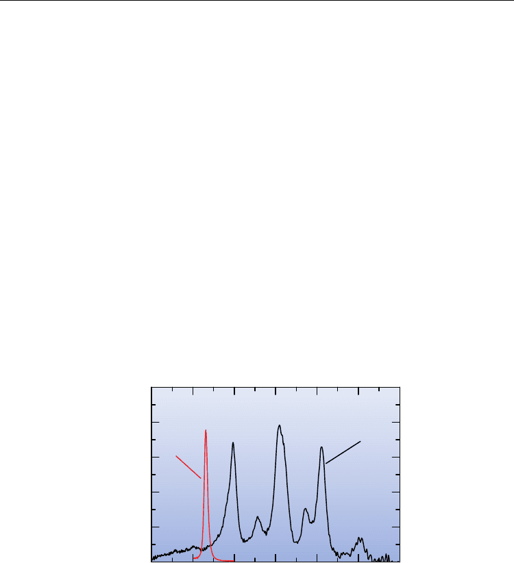
Electronic Properties of Carbon Nanotubes
354
spectrum from micelle encapsulated SWNTs dispersed in D
2
O solution. The many PL
peaks arising from various types of SWNTs with different chirarities (diameters) are
observed in the macroscopic PL spectrum. The optically excited e-h pair in SWNTs forms
bound hydrogen like exciton state due to strong Coulomb interaction and recombination
of exciton (not free e-h pair) is the origin PL signals in the SWNTs. The shape of each PL
(or absorption) peak contains physical information including the exciton dynamics. The
shape of ensemble averaged PL spectrum shows the near Gaussian function, which means
that each SWNT with same chiral indicies is in the different environment (local strain,
dielectric constant, and ....). The exciton transition (absorption and PL) of each SWNT is
affected from the Gaussian distributed inhomogeneous environment, causes fluctuation of
the energy. The PL broadening arising from the inhomogenity is called as
“inhomogeneous broadening”, which covers the intrinsic optical and electronic properties
of SWNTs. In contrast, the effect of the inhomogeneous broadening is eliminated in the PL
spectra from a single SWNT (red line in Fig. 1). The sophisticated optical spectroscopic
technique, called as a single carbon nanotube spectroscopy, enables us to observe PL
spectrum from a single SWNT (Hartschuh et al., 2003, Htoon et al., 2003, Lefebvre et al.,
2004, & Matsuda et al., 2005). The red solid line of Figure 1 shows the PL spectrum from a
single SWNT. The PL of a single SWNT shows very clear single peak and very narrow
linewidth, which provide us the fruitful information of intrinsic properties of SWNT. The
intrinsic linewidth in the PL spectrum of a single SWNT is called as homogeneous
linewidth. The homogeneous linewidth contains the dynamical properties of exciton in
the SWNT, discussed after in detail.
0.8 0.9 1.0 1.1 1.2 1.3 1.4
Photon Energy (eV)
ensemble
single
PL Intensity (arb. units)
Fig. 1. Ensemble averaged PL spectrum (balck solid line) and PL spectrum of a single SWNT
(red line).
2.1 Homogeneous linewidth broadening of optical spectrum
In the quantum two-level systems, the optical spectra broaden and have finite linewidths
due to finite lifetime of the excited state according to the Heisenberg relationship. There are
two kinds of excited state lifetime, energy relaxation time T
1
and phase relaxation
(dephasing) time T
2
. In the molecular systems, the phase relaxation of the excited state