Marulanda J.M. (ed.) Electronic Properties of Carbon Nanotubes
Подождите немного. Документ загружается.


Geometric and Spectroscopic Properties of Carbon Nanotubes and Boron Nitride Nanotubes
185
in the (12,0)-SWCNT spectrum are respectively blue-shifted to 525 cm
-1
and 276 cm
-1
in the
Raman spectrum of (6,0)&(12,0)-DWCNT. Additionally, the RBMs for (7,0)-SWCNT (410 cm
-
1
) and (14,0)-SWCNT (214 cm
-1
) are respectively upward shifted to 450 cm
-1
and 237 cm
-1
in
the spectrum of (7,0)&(14,0)-DWCNT. The relative distances between RBMs in the spectrum
of (n,0)&(2n,0)-DWCNTs are larger than the distances between corresponding RBMs in
Raman spectra of (n,0)- and (2n,0)-SWCNTs. Even though we do not have enough data for
the calculated RBMs for different sized DWCNTs, a tentative equation for the RBMs may be
given by equations below;
ω
RBM
62cm
.
.
(3.3.9a)
ω
RBM
45cm
.
.
(3.3.9b)
Where d
t
stand for the shell diameter. In the high frequency region, Figure 5 provides the
calculated Raman modes (with E
1g
/ A
1g
/ E
2g
symmetries). When we compare these
tangential bands with their band position in the corresponding SWCNT spectra, it can be
seen that they are downward shifted (relative to SWCNTs). The animations of the normal
modes showed that the strong Raman peaks are mostly resulting from the nuclear motions
of the outer-shell.
3.4.1 (n,0)- and (n,n)-boron nitride nanotube
Blase et al [98] have theoretically studied the possibility of obtaining boron nitride nanotubes
(BNNTs) and initiated an exploration on their characteristic properties [99,100,101], by
investigating the connection between hexagonal boron nitride sheets [102] and graphite.
Even though a hexagonal boron nitride sheet is made up of alternating atoms of boron and
nitrogen, boron nitride surprisingly yields atomic structures like those of graphite.
Moreover, the crystallographic parameters of hexagonal boron nitride sheets and graphite
are nearly identical. Like CNTs, BNNTs with different chiralities can be formed by rolling
up a hexagonal sheet of boron nitride in different chiral directions.
BNNTs have many properties similar to those of CNTs [103,104]. For example, chemical
inertness [105], high heat conduction, piezoelectricity [106], exceptional elastic properties
[107,108,109,110], high mechanical strength [111,112,113,114],and diameter dependence of
the Raman bands [99]. In contrast, whereas CNTs are highly toxic for the human body, and
can be semiconductors and conductors depending on their chirality, BNNTs show good
biocompatibility and are always semiconducting with a large band gap [99], regardless of
their chirality.
The diameter dependence of the vibrational frequency of SWBNNTs has been investigated
by many researchers [115]. Sanchez-Portal and Hernandez [116] calculated the dependence
of the vibrational properties of the SWBNNTs using TB approximation. By using first
principles, Wirtz and Rubio [117] calculated the phonon-dispersion relation for Raman and
infrared active modes of (n,0)- and (n,m)-type of the BNNTs. A comparative study of the
radial breathing mode was also conducted [118] showed that the frequencies of BNNTs are
lower than those of CNTs whose diameter are close to that of BNNTs. Furthermore, the
surface buckling that is sole to BNNTs was observed in consequence of the different
hybridizations of boron and nitrogen in the bent nanotube surfaces [108,117,119]. Even
though numerous theoretical studies have been done on the diameter dependence of the

Electronic Properties of Carbon Nanotubes
186
RBM modes of frequency, a systematic study has not yet been undertaken, although BNNTs
has applications in a broad range of fields, such as nanoresonators, nanosensors, actuators
and transducers. [120,121,122]. Up to now, SWBNNTs have been especially considered as
circular nano-cylinders like SWCNTs. However, Chowdhury et al[99] pointed out that this
may not be always true as the iconicity of the BN bonds responsible for the surface buckling
in hoop direction, could also lead to distortion of the optimized configuration in the axial
direction when BNNTs are used with practical end constraints.
The present work aims to achieve a realistic configuration of the optimized SWBNNTs
structure, and conduct a detailed study on geometric and spectroscopic properties. These
properties include diameter dependence of the Raman and IR spectra of SWBNNTs at same
level of the density functional theory (DFT) as used for SWCNTs.
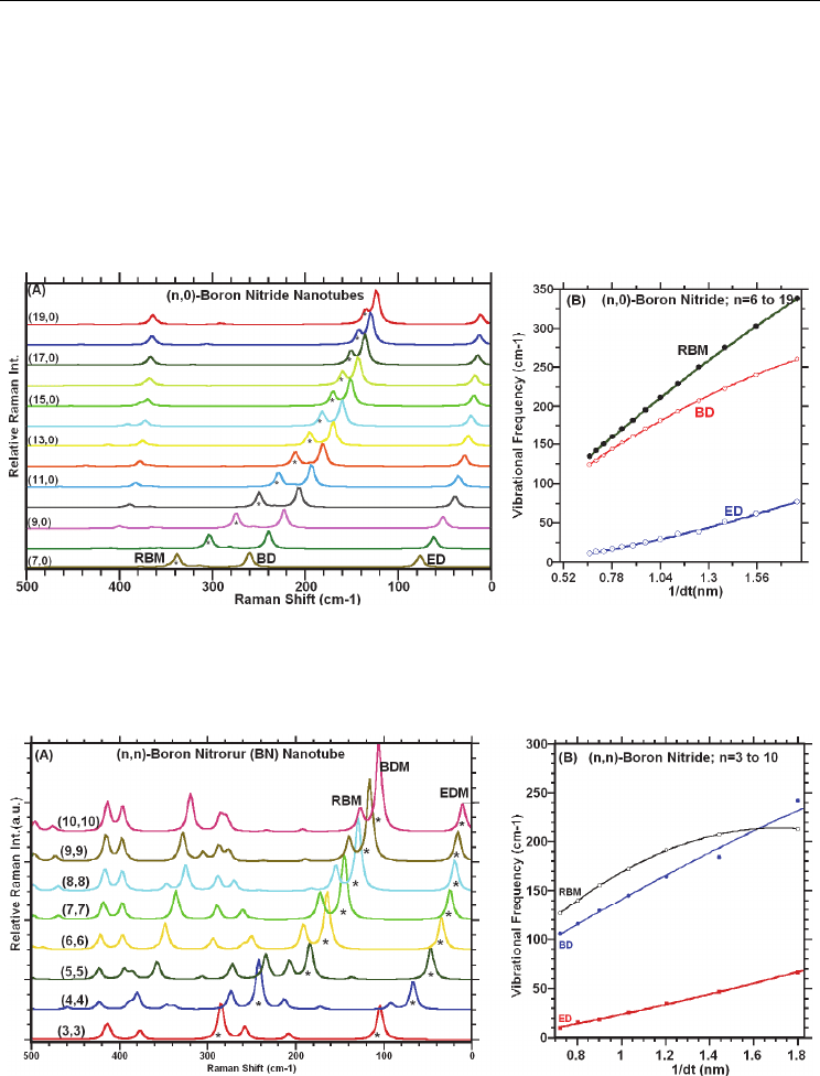
3.4.2 Raman spectra of the (n,0)- and (n,n)-SWBNNTs
We calculated the spectroscopic and geometric parameters of the (n,0)-SWBNNTs with n = 7
to 19 and (n,n)-SWBNNTs (n=3 to 10) at the same level of the DFT used for the SWCNTs.
The assignments to motions of atoms or groups of atoms have been carried out through use
of vibration visualization software (GaussView03) that is similar to the assignment made for
the (n,0)-SWCNTs as seen in Table 3.3.1, and therefore, are given here. As found for the
CNTs, the calculated Raman spectra of the (n,0)- and (n,n)-SWBNNTs in the low frequency
region indicated that three of the Raman bands of frequencies are strongly diameter
dependent. If the motion of the boron and nitrogen atoms within the nanotube is due to the
stretching of the BNNT along its diameter, this result in an elliptical shape abbreviated as
ED mode. If it is due to the bending deformation of the BNNT, which results from
expansion of the nanotube along diagonal axis, with the motion of two end groups being in
opposite directions, this is abbreviated as ED mode. Finally, if the motion of the atoms is in
the radial direction in the same phase, this is referred to radial breathing mode, RBM. The
calculations exhibited by these Raman bands are also strongly diameter dependent as
shown in Figure 3.4.1A-B and Figure 3.4.2A-B for the (n,0)- and (n,n)-SWBNNTs,
respectively. The best fit were obtained using a quadratic fitting equation, given by Eq.
3.4.1a-c and Eq. 3.4.2a-c for the (n,0)- and (n,n)-SWBNNTs, respectively. These reproduced
the calculated RBMs within ~ 0.6 cm
-1
error ranges, when compared to their corresponding
calculated Raman spectra by the DFT technique.
RBM
,
14.34
..
.
.
(3.4.1a)
BD
,
0.51
..
.
.
(3.4.1b)
ED
,
9.81
..
.
.
(3.4.1c)
RBM
,
27.51
..
.
.
(3.4.2a)
BD
,
1.09
..
.
.
(3.4.2b)
ED
,
17.13
..
.
.
(3.4.2c)
Geometric and Spectroscopic Properties of Carbon Nanotubes and Boron Nitride Nanotubes
187
Furthermore, as mentioned in Section 3.3.1, the calculated BD band for (n,0)-SWCNTs is not
only diameter dependent, but is also dependent on whether the number of hexagons formed
in the circumference direction of the SWCNTs (0,2n) type or (0,2n+1) type, respectively are
even or odd. However, the calculated ED band for the SWBNNTs did not exhibit
dependence on even and odd number of the hexagon in the circumference direction of the
(n,0)-SWBNNTs. Moreover, as seen in Figure 3.4.1A-B and 3.4.2A-B, for large sized
SWBNNTs, the ω
and ω
mode frequencies converge. The calculated frequency
separation between the RBM and BD to found to be 11 cm
-1
for the (19,0)-SWBNNT and 20
cm
-1
for the (10,10)-SWBNNTs. It should be noticed that the RBM and BD bands would have
unresolvable for the (n>20,0)-SWBNNT, such that found for the (n,0)-SWCNTs.
Fig. 3.4.1. Calculated Raman spectra: (A) increased resolution in the low frequency region,
showing diameter dependence of the calculated Raman band frequencies for the (n, 0)-
SWBNNTs, n = 7 to 19; (B) the plots of the frequencies of vibrational modes (ED, BD and
RBM) versus 1/dt.
Fig. 3.4.2. Calculated Raman spectra:
(A) increased resolution in the low frequency region,
showing diameter dependence of the calculated Raman band frequencies for the (n, n)-
SWBNNTs, n = 3 to 10;
(B) the plots of the frequencies of vibrational modes (ED, BD and
RBM) versus 1/dt.
Electronic Properties of Carbon Nanotubes
188
We can anticipate, as mentioned earlier for the (n,0)-SWCNTs, in general, that the
acquisition of Raman spectra for experimental samples consisting of large diameter
SWBNNT with the purpose of characterizing the sample in terms of electronic properties
and purity may be complicated by the existence of this BD band, which can lead to apparent
broadening of bands as well as the presence of additional bands that may lead to the
erroneous conclusion that more than one type of the nanotube is present in the sample.
Also, we have found that calculated Raman bands of the (n,0)- and (n,n)-SWBNNTs in the
mid-frequency region (500-1000 cm
-1
) exit almost diameter-independent peak positions.
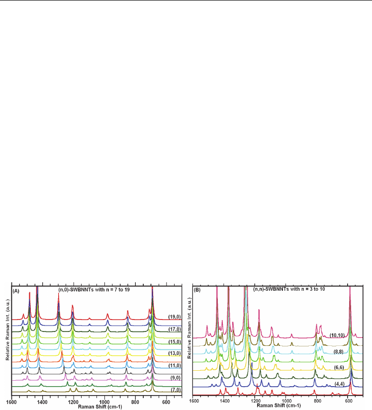
While, as seen in Figure 3.4.3A, in the high-frequency region there are three major Raman
bands that are diameter-dependent; two of them lie between 1400-1550 cm-1 region and
another one lie between 1200-1300 cm-1 region. However, the Raman peaks at about 1200
cm-1 remain almost constant. The latter two Raman approach one another with decreasing
the tube diameter. For the (n,n)-SWBNNTs, the pattern of the Raman peak in the region of
1000-1550 cm
-1
are similar to these of the (n,0)-SWBNNTs. While the Raman peak at about
1170 cm-1 remain almost constant, the other major peaks indicated the dependence on the
diameter of the (n,n)-SWBNNTs as shown in Figure 3.4.3B. As discussed earlier, the
curvature energy (as given by Eq. 3.1.1) of the nanotube brings about dissimilar force
constants along the nanotube axis and the circumference direction. Therefore, the nanotube
geometry causes a force constant reduction along the tube axis compared to that in the
circumferential direction. As a result, based on the calculations, the curvature effect might
play a crucial role in the shift of the peak positions of the G-band as well as the RBM band.
Furthermore, It should be noticed that these three major peaks (in the region of ~1200-1500
cm
-1
) consist of more than one Raman peak with the different symmetry like A
g
and E
g
.
Fig. 3.4.3. Calculated Raman spectra: increased resolution in the high frequency region,
showing diameter dependence of the calculated Raman band frequencies:
(A) for the (n, 0)-
SWBNNTs, n = 7 to 19 and
(B) for the (n, n)-SWBNNTs, n = 3 to 10.
Since the atomic motion for each symmetry is in different directions, one (for instance, with
symmetry of A
g
or E
g
) might be enhanced or slightly shifted by a functional group
connected to the nanotube by means of covalently bonding or electrostatic interactions. This
enhancement or shift in the Raman active peak(s) position might provide some useful
information about the structure of functionalized-nanotube, for instance, which of the side
of a given functional group covalently bonded or interacts with the nanotube surface or
functional group attached to the nanotube along the tube axis or perpendicular to it. This is

Geometric and Spectroscopic Properties of Carbon Nanotubes and Boron Nitride Nanotubes
189
important because the absorption of the nanotube in the perpendicular direction is much
greater than absorption in the parallel direction; therefore, the availability of photons with
polarization parallel to the nanotube axis is greater than that of photons with polarization
perpendicular to it. It means that nanotube creates a local electric field aligned along the axis
of the nanotube and facilitating the interaction of functional group with the nanotube. Even
it may provide charge transfer mechanism for the functionalized-nanotube as the charge
transfer from nanotube to molecule as observed between the molecule and nanoparticles by
surface enhanced Raman spectroscopy (SERS).[123]
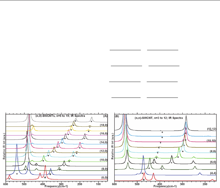
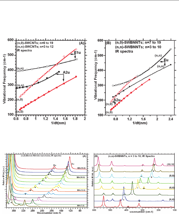
3.5.1 IR spectra of (n,0)- and (n,n)-SWCNTs/SWBNNTs
Figures 3.5.1A-B provide calculated IR spectra for the (n,0)- and (n,n)-SWCNTs, respectively,
where n ranges from 6 to 19 for the zigzag and from 3 to 12 for the armchair nanotube. As
evidenced in Figure 3.5.1A-B, there are two IR active vibrational modes, of A
2u
and E
1u
symmetries, whose frequencies are strongly diameter dependent. Least squares fits to the
computed frequencies as functions of diameter for the zigzag- and armchair-SWCNTs are
shown in Figure 3.5.2A. The fit to the data, for the two bands (of A
2u
and E
1u
symmetries)
are respectively given by Eqs. 3.5.1a-b for the zigzag- and by the Eqs. 3.5.1c-d for the
armchair-SWCNTs. The principal motions these bands correspond to, have been
determined by the visualization software mentioned earlier. For the A
2u
band, the wagging
of the SWCNT is along its radial direction, where the motion of the two end groups move in
opposite directions. For the E
1u
band, the principal motion involves wagging of the SWCNT
along its circumference direction. Our short hand notation for these two principal vibrations
are the subscripts shown on the frequencies, where RW and CW, respectively, specify radial
and circumference wagging.
ω
A
;n,01.85
..
.
.
(3.5.1a)
ω
E
;n,07.33
..
.
.
(3.5.1b)
ω
A
;n,n265.42
..
.
.
(3.5.1c)
ω
E
;n,n367.66
..
.
.
(3.5.1d)
It is to be noted (for completeness sake), that in the high frequency vibrational region of
Figure 3.5.1A-B, as revealed upon close inspection, there are three IR vibrational mode of
frequencies ~1520 cm
-1
(E
1u
symmetry), ~1365 cm
-1
(E
1u
) and ~1332 cm
-1
(A
2u
) whose
positions show weak dependence on diameter; additionally, in the mid frequency region,
there is one IR-mode of frequency ~780 cm
-1
(A
2u
) that is also weakly diameter dependent.
Hence, the strong diameter dependence of the two low frequency bands may be useful for
determining structural indices of SWCNT samples. A more detailed description of the
assignments for bands in the IR spectra for the various (n,0)-SWCNTs is contained in Table
3.5.1.
Figure 3.5.3A-B provide the calculated IR spectra of the zigzag-(n,0) and armchair-(n,n)
single-wall boron nitride nanotube (SWBNNTs) exhibits similar band structure to their
corresponding SWCNTs with the same chiral index (n,0) and (n,n), when comparing the
Electronic Properties of Carbon Nanotubes
190
calculated IR spectra of the (n,0)- and (n,n)-SWBNNTs with the (n,0)- and (n,n)-SWCNTs
(see Figure 3.5.1A-B). Least squares fits to the computed frequencies as functions of
diameter for the zigzag- and armchair-SWBNNTs are shown in Figure 3.5.2B. The fits to the
data, for the two bands (
ω
and ω
) are respectively given in Eqs. 3.5.2a-b for the (n,0)-
and given in the Eqs. 3.5.2c-d for the (n,n)-SWBNNTs.
ω
A
;n,012.40
..
.
.
(3.4.2a)
ω
E
;n,038.67
..
.
.
(3.4.2b)
ω
A
;n,n104.50
.
.
.
.
(3.4.2c)
ω
E
;n,n298.17
..
.
.
(3.4.2d)
Fig. 3.5.1 Calculated IR spectra (A) for the (n,0)-SWCNTs, with n varying from 0 to 19; (B)
for the (n,n)-SWCNTs with n = 3 to 12. Where signs * and + stand for the IR active modes of
frequencies;
ω
A
and ω
A
, respectively.
Furthermore, for DWCNTs (not shown here), the calculated IR bands with A
2u
symmetries
at 387 and 216 cm
-1
for (0,6)- and (0,12)-SWCNTs are blue-shifted to 395 and 253 cm
-1
in IR
spectrum of (0,6)&(0,12)-DWCNTs, respectively. The IR bands with A
2u
symmetries at 358
and 187 cm
-1
in spectra of (0,7)- and (0,14)-SWCNTs correspond to the bands at 411 and 247
cm
-1
in spectrum of (0,7)&(0,14)-DWCNT. Furthermore, the IR bands with E
1u
symmetries at
580 and 339 cm
-1
for (0,6)- and (0,12)-SWCNTs are also blue-shifted to 617 and 350 cm
-1
in
the spectrum of (0,6)&(0,12)-DWCNT, respectively. The bands (with E
1u
symmetries) at 541
and 295 cm
-1
in spectra of (0,7)- and (0,14)-SWCNTs correspond to the bands at 567 and 300
cm
-1
in the spectrum of (0,7)&(0,14)-DWCNT, respectively.
3.6.1 Calculated vertical transitions of the SWCNTs and SWBNNTs
As mentioned earlier in Section 2, the chiral index (n,m) of the nanotube indicates whether
the tube is metallic or semiconducting. When the (n-m) = 3q (q = 0, 1,2 ,3 …), all the tubes
are metallic, if not , semiconducting. Therefore, all armchair tubes are metallic. The
calculated density of states (DOS) of the nanotube using tight binding approximation (TBA)
Geometric and Spectroscopic Properties of Carbon Nanotubes and Boron Nitride Nanotubes
191
does not comprise one smooth band, but shows a number of side-bands with spikes around
the Fermi level separated from each other [92,124], which are called the van Hove
singularities. The side-bands represent 1D channel for conduction along the nanotube. The
side-bands and their sharp onsets have been observed in their tunneling DOS obtained from
scanning tunneling spectroscopic measurements [125].
Fig. 3.5.2 The plots of the dependence of calculated IR frequencies, in the low frequency
region, as a function of nanotube diameter for vibrational modes of symmetries A
2u
and E
1u
;
(A) for the SWCNTs and (B) for the SWBNNTs.
Fig. 3.5.3
(A) Calculated IR spectra of the (n,0)-SWNTs, with n varying from 7 to 19; (B)
illustrate for the (n,n)-SWBNNTs with n = 3 to 10.
For larger-diameter tubes, the singularities move close together and combine, thus making
the DOS similar to that of a graphene layer. In contrast, for smaller-diameter nanotubes, the
singularities are well separated specially near the Fermi level and can give initial and final
states for a resonance Raman scattering (RRS) process. In a simplified representation,
neglecting all the curvature effects and considering the linear dispersion of π and π* bands

Electronic Properties of Carbon Nanotubes
192
of graphene only, the energy gap between q
th
van Hove singularity in valence and
conduction bands for metallic tubes[126] is
3
1,2.3,…. ) and
for semiconducting tubes as discussed in Section 2. In the case of metallic tubes,
the linear crossing of π and π* bands near the Fermi level yields a small constant DOS
leading to sharp van Hove singularities at energies away from the Fermi energy. In contrast,
for semiconducting tubes, the DOS at Fermi energy is zero with sharp van Hove
singularities away from the Fermi energy [92,127].
The electronic structures of the SWBNNTs were theoretically investigated by Rubio et al.
[56] using the tight binding approximation (TBA). All SWBNNTs were found to be
semiconducting materials with band gaps larger than 2 eV. BNNTs with larger diameters
have a larger band gap, with a saturation value corresponding to the band gap of a
hexagonal boron nitride (BN) as calculated by Rubio et al.[56] or see the Figure 4 in Ref.[57].
The subsequent studies based on local-density-functional (LDA) calculations proved that it
is energetically more favorable to fold a hexagonal boron nitride sheet into a BNNT than to
forma CNT from a graphite sheet [58]. This observation is also supported by our
calculations at B3LYP/6-31G level of DFT as discussed in Section 3. Based on the band-
folding analysis, SWBNNTs are semiconductors with large-gap for the zigzag- and
armchair-SWBNNTs. This is due to the strong hybridization effects may take place because
tube curving reduces the BNNT’s band gap remarkably. For the (n, 0) BNNTs, with n > 12
the hybrid state was found not to play any role in determining tube gaps. The gaps are
steady at around 4 eV as indicated by LDA. In another calculation using density functional
theory, the band gaps of BNNTs were eventually saturated at 5.03 eV with an increase in
diameter [128,129,130,131,132]. Based our calculated dipole allowed vertical electronic
transitions, for the (n, 0)-BNNTs with n > 11, the gabs are steady around 5.9 eV, see Figure
3.6.1B and Table 3.6.4. For the (n,n)-SWBNNTs, with n>10, the band gaps slightly increases
with increasing tube diameter and seem to be steady at around 5.84 eV according to our
DFT calculations as seen Figure 3.6.1B and Table 3.6.4. It should be noted that there are
many forbidden electronic transition lie below the allowed one. Based on our experience on
the calculated electronic transitions for many organic compounds at B3LYP level and at the
BLYP level of DFT for the transition metals [95], the calculated value of the electronic
transitions are somewhat higher than their experimental values, as much as 0.4 eV.
Therefore, the calculated values of the electronic band gabs for the nanotubes might be
reasonable.
Various methods have been developed to tune the electronic structure of BNNTs is nicely
discussed by Chunyi Zhi et al.[57], for instance, applying electric field
[133,134,135,136,137,138] or strain [139], or chemical methods, like doping [140,141,142,67],
introducing defects [143,144,145] or surface modification [60,146,147]. The methods and
species chosen are summarized in Table 2 in Ref. 57. Physical methods could directly reduce
the band gap of BNNTs, while chemical methods were found to tune the band gap by
introducing localized energy levels inside the gap [57]. For example, by applying an 2 V/nm
electric field, the band gap of a (12, 12) BNNT was directly reduced from 4.5 eV to about 2.5
eV [135], while F-doping induced an unoccupied localized state in the gap of BNNTs [148].
In addition, chemical modification methods of BNNTs were sometimes found to enrich the
properties of BNNTs, for instance, polarization field was induced by chemical adsorption
[149] or ferromagnetism appeared in doped BNNTs.

Geometric and Spectroscopic Properties of Carbon Nanotubes and Boron Nitride Nanotubes
193
For electronic structure of multi-walled BNNTs (MWBNNTs), it has been reported that there
is hybridization between p and s states of inner and outer tubes [150,151]. This effect leads
to the top valence and bottom conduction bands localization on the outer and inner tubes,
respectively [57]. The band gap of DWBNNTs is slightly narrower than that of the inner
tubes. This is because the downward shifts of the p states of the inner tube are larger than
those of the outer tube. Furthermore, in the interwall region the peculiar charge
redistribution is induced by the near-free-electron states of BNNTs [57,152]. The fluorine
doping can significantly modify the DWBNNTs’ inter-wall interactions and thus both tube
walls turn into effective conducting channels. This leads to a remarkably improved electrical
transport in them [151].
There are strong interactions between electrons and holes in BNNTs [54,55]. The excitonic
effects were indeed shown to be more important in BNNTs than in CNTs. Bright and dark
excitons in BNNTs alter the optical response qualitatively. For example, the absorption
spectrum of the (8, 0) BNNT is dominated by a peak at 5.72 eV, due to an exciton with a
binding energy of 2.3 eV. The binding energy for the first excitonic peak is more than 3 eV
for the (2, 2) nanotube, which will fast converge to around 2.1 eV of the hexagonal single BN
sheet as a result of strongly localized nature of this exciton [57], which is consistent with the
results by the Louie’s group [54]: a 2.3 eV binding energy for a (8, 0) BNNT.
In this section, we provided the calculated vertical electronic transitions of the (n,0)- and
(n,n)-type nanotubes using time-dependent DFT methods at the TD-B3LYP/6-31G level.
Table 3.6.1 and Table 3.6.2 provide the calculated electronic transitions from (7,0) to (11,0)
and (14,0) and from (3,3) to (10,10) for the SWCNTs, respectively. The transitions from the
(7,0) to (14,0) and from (3,3) to (10,10) for the zigzag- and armchair-SWBNNTs are given in
Table 3.6.3 and Table 3.6.4, respectively.
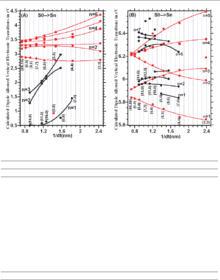
The diameter dependence of the calculated dipole allowed electronic transitions are shown
in Figure 3.6.1A-B. As seen in Figure 3.61A, the allowed electronic transitions lie in the range
from 0.5 eV to 3.0 eV for the (n,0)-SWCNTs, with n = 7 to 14, and lie in the range from 2.8 eV
to 4.4 eV for the (n,n)-SWCNTs, with n=3 to 10. Furthermore, the plot of the calculated
dipole allowed electronic transitions showed that while the allowed transitions rapidly
decrease and stabilize (around 0.5 eV) with increasing the diameter of the (n,0)-SWCNTs, for
the armchair SWCNTs, the electronic transitions are diameter dependent, but also these
transitions converge and become constant (around 3 eV) with increasing tube diameters of
the (n,n)-SWCNTs. For the SWBNNTs, the result of the calculations indicated that the dipole
allowed electronic transitions are not only diameter dependent, but also the electronic
transitions lie in the range from 5.7 eV to 6.6 eV as seen in Figure 6.3.1B, which is higher
than the calculated electronic transitions for the SWCNTs. This large band gap in SWBNNTs
relative to SWCNTs is not so surprising since the B-N bond contains a significant ionic
component. This polarity can extremely alter both molecular and solid-state electronics as
well as optical properties of the system by modifying the character of the frontier molecular
orbitals [57]. Furthermore, the calculated band gap of BNNTs between 5.7 and 6.6 eV is
independent to tube chirality. This provides good electrical insulation, in spite of the fact
that CNTs can be a metal or a narrow band-gap semiconductor. This discrepancy in
electronic structure results in different luminescence emission: SWBNNTs have violet or
ultraviolet luminescence under excitation by electrons or photons, while SWCNTs can emit
infrared light and the wavelengths depend on their chiralities.
Electronic Properties of Carbon Nanotubes
194
Fig. 3.6.1. Diameter dependence of calculated dipole allowed vertical electronic transitions
of: a) SWCNTs and b) SWBNNTs at B3LYP/6-31G level of DFT.
(7,0) (8,0) (9,0) (10,0) (11,0) (14,0)
m TB DFT
f TB
DFT
f TB
DFT
f TB
DFT
f TB
DFT
f TB
DFT
f
1
0.91 1.04
0.77
0.02
0.56
1.10
0.64
0.01
0.36
0.758
0.50 0.0042
2
1.25 1.46
0.80
1.09
0.51
0.63
3
1.25 1.46
0.80
1.09
0.52
0.63
4
1.42
1.45 0.06
2.44
0.93
0.04
1.77
0.98
0.58
0.02
0.89
5
2.52 2.40
2.51
0.36
2.32
2.04
1.80
1.10
6
2.53 2.51
0.36
2.32
2.04
1.80
1.10
7
2.93 2.53
2.50
2.20
2.14
0.50
1.78
1.97
0.50
1.29 0.0872
8
2.93 2.00
2.50
2.14
0.50
1.97
0.50
1.436
1.65 0.7917
9
3.02 2.78
2.64
2.23
0.12
2.06
0.12
1.65 0.7925
10
3.02 2.78
2.64
2.53
2.06
1.95
11
3.08 2.77
2.72
2.75
2.14
1.96
12
3.08 2.98
0.13
2.72
2.75
2.14
2.20
dt
0.56 0.64
0.71
0.79
0.87
1.10
Table 3.6.1. DFT-calculated vertical singlet–singlet transitions (
→
in eV) of the (n,0)-
SWCNTs, n = 7 to 11, at the B3LYP/6-31G level. Oscillator strengths (f) and results of the
calculated energy from the tight-binding (TB) approximation for each nanotube are
provided for comparison. The value of was taken to be 2.7 eV in the TB calculations. The d
t
stands for diameter in nm.