Lallart M. (ed.) Ferroelectrics - Physical Effects
Подождите немного. Документ загружается.


Compositional and Optical Gradient in Films of PbZr
x
Ti
1-x
O
3
(PZT) Family
599
Fried, M.; Petrik, P.; Lohner, T.; Khánh, N. Q.; Polgár O.; Gyulai, J. (2004), Dose-dependence
of ion implantation-caused damage in silicon measured by ellipsometry and
backscattering spectrometry. Thin Solid Films 455-456, 404
Gibbons, B.J.; Trolier-McKinstry, S. (1999), The sensitivity limits of spectroscopic
ellipsometry to oxygen content in YBa2Cu3O7-d thin films. Thin Solid Films 352, 205
Gkotsis, P.; Kirby, P.B.; Saharil, F.; Oberhammer, J.; Stemme, G. (2007), Thin film crystal
growth template removal: Application to stress reduction in lead zirconate titanate
microstructures. Applied Physics Letters, 91, 163504
Glinchuk, M. D.; Eliseev, E. A.; Deineka, A.; Jastrabik, L. (2000), Optical refraction index and
electric polarization profile of ferroelectric thin film. Fine mechanics and optics, 45,
338-342
Glinchuk, M. D.; Eliseeva, E.A.; Stephanovich, V.A. (2002), The depolarization field effect on
the thin ferroelectric films properties. Physica B, 322, 356–370
Guenther, M.; Gerlach, G.; Suchaneck, G.; Sahre, K.; Eichhorn, K.-J.; Wolf, B.; Deineka, A.;
Jastrabik, L. (2002), Ion-beam induced chemical and structural modification in
polymers. Surface and Coatings Technology, 158-159, 108
Gusmano, G.; Bianco, A.; Viticoli, M.; Kaciulis, S.; Mattogno, G.; Pandolfi, L., (2002), Study of
Zr
1−x
Sn
x
TiO
4
thin films prepared by a polymeric precursor route. Surface and
Interface Analysis, 34, 690–693
Impey, S. A.; Huang, Z.; Patel, A.; Beanland, R.; Shorrocks, N. M.; Watton, R.; Whatmore, R.
W. (1998), Microstructural characterization of sol-gel lead-zirconate-titanate thin
films. Journal of Applied Physics, 83, 2202
Izyumskaya, N.; Alivov, Y.-I.; Cho, S.-J.; Morkoc, H.; Lee, H.; Kang, Y.-S. (2007), Processing,
Structure, Properties, and Applications of PZT Thin Films. Critical Reviews in Solid
State and Materials Sciences, 32, 111-202
Jellison, G. E.; Modine, F. A. (1996), Parameterization of the optical functions of amorphous
materials in the interband region. Applied Physics Letters, 69, 371
Jellison, G. E.; Modine, F. A.; Boatner, L. A. (1997), Measurement of the optical functions of
uniaxial materials by two-modulator generalized ellipsometry: rutile (TiO
2
), Optics
Letters, 22
, 1808
Kamp, D. A.; DeVilbiss, A. D.; Philpy, S. C.; Derbenwick, G. F. (2004), Adaptable
ferroelectric memories for space applications. IEEE, Non-Volatile Memory
Technology Symposium 2004, 10.1109/NVMT.2004.1380832
Lappalainen, J.; Hiltunen, J.; Lantto, V. (2005), Characterization of optical properties of
nanocrystalline doped PZT thin films. Journal of European Ceramic Society, 25, 2273
Ledermann, N. ; Muralt, P. ; Baborowski, J.; Gentil, S.; Mukati, K.; Cantoni, M.; Seifert, A.;
Setter, N. (2003), {1 0 0}-Textured, piezoelectric Pb(Zr
x
, Ti
1−x
)O
3
thin films for
MEMS: integration, deposition and properties. Sensors and Actuators A, 105, 162–170
Losurdo, M. (2004), Relationships among surface processing at the nanometer scale,
nanostructure and optical properties of thin oxide films. Thin Solid Films, 455-456,
301
Marcus, R. K.; Schwartz, R. W. (2000), Compositional profiling of solution-deposited lead
zirconate–titanate thin films by radio-frequency glow discharge atomic emission
spectroscopy (rf-GD-AES), Chemical Physics Letters, 318, 481–487
Martin, M. (2003), Materials in thermodynamic potential gradients. Journal of Chemical
Thermodynamics, 8, 1291–1308.

Ferroelectrics – Physical Effects
600
Morita, T.; Kanda, T.; Yamagata, Y.; Kurosawa, M.; Higuchi, T. (1997), Single process to
deposit lead zirconate titanate (PZT) thin film by a hydrothermal method. Japanese
Journal of Applied Physics, 36, 2998
Morozovskaa, A. N.; Eliseevb, E. A.; Glinchuk, M. D. (2007), Size effects and depolarization
field influence on the phase diagrams of cylindrical ferroelectric nanoparticles.
Physica B, 387, 358–366
Morton, D. E.; Johs B.; Hale, J. (2002), Soc. of Vac. Coat. 505/856-7188, 45th Ann. Techn. Conf.
Proc. ISSN 0737-5921, 1
Muralt, P. (2000), Ferroelectric thin films for micro-sensors and actuators: A review.
IOPscience::.. Journal of Micromechanics and Microengineering, 10, 136-146
Nguyen Van, V.; Brunet-Bruneau, A.; Fisson, S.; Frigerio, J. M.; Vuye, G.; Wang, Y.; Abelνs,
F.; Rivory, J.; Berger, M.; Chaton, P. (1996), Determination of refractive-index
profiles by a combination of visible and infrared ellipsometry measurements.
Applied Optics, 35, 5540
Nishizawa, H.; Tateyama, Y.; Saitoh, T. (2004), Ellipsometry characterization of oxidized
copper layers for chemical mechanical polishing process. Thin Solid Films, 455-456,
491
Ohba, Y.; Arita, K.; Tsurumi, T.; Daimon, M. (1994), Analysis of interfacial phase between
substrates and lead zirconate titanate thin films synthesized by hydrothermal
method. Japanese Journal of Applied Physics, 33, 5305
Okamura, S.; Miyata, S.; Mizutani, Y.; Nishida, T.; Shiosaki, T. (1999), Conspicuous voltage
shift of D–E hysteresis loop and asymmetric depolarization in Pb-based
ferroelectric thin films. Japanese Journal of Applied Physics, 38, 5364–5367
Okamura, S.; Miyata, S.; Mizutani, Y.; Nishida, T; Shiosaki, T. (1999), Conspicuous voltage
shift of D–E hysteresis loop and asymmetric depolarization in Pb-based
ferroelectric thin films. Japanese Journal of Applied Physics, 38, 5364–5367
Oulette, M. F.; Lang, R. V; Yan, K. L.; Bertram, R. W.; Owle, R. S.; Vincent, D. (1991),
Experimental studies of inhomogeneous coatings for optical applications. Journal of
Vacuum Science and Technology A, 9, 1188- 1192
Parish, C. M.; Brennecka, G. L.; Tuttle, B. A.; Brewer, L. N. (2008), Quantitative X-Ray
Spectrum Imaging of Lead Lanthanum Zirconate Titanate PLZT Thin-Films. Journal
of American Ceramic Society
, 91, 3690
Philpy, S. C.; Kamp D. A.; Derbenwick G. F. (2003), Hardened By Design Ferroelectric
Memories for Space Applications,” Non-Volatile Memory Technology Symposium
2003, San Diego, California
Reaney, I. M.; Taylor, D. V.; Brooks, K. G. (1998), Ferroelectric PZT thin films by sol-gel
deposition. Journal of Sol-Gel Science and Technology, 13, 813
Rivory, J. (1998), Characterization of inhomogeneous dielectric films by spectroscopic
ellipsometry. Thin Solid Films, 313-314, 333
Snyder, P.G.; Xiong, Y.-M.; Woollam, J.A.; Al-Jumaily G.A.; Gagliardi, F.J. (1992), Graded
refractive index silicon oxynitride thin film characterized by spectroscopic
ellipsometry. Journal of Vacuum Science and Technology A, 10, 1462
Sternberg, A.; Krumins, A.; Kundzins, K.; Zauls, V.; Aulika, I.; Cakare, L.; Bittner, R.; Weber,
H.; Humer, K.; Lesnyh, D.; Kulikov D.; Trushin, Y. (2003), Irradiation effects in lead
zirconate thin films. Proceedings of SPIE, 5122, 341

Compositional and Optical Gradient in Films of PbZr
x
Ti
1-x
O
3
(PZT) Family
601
Suchaneck, G.; Lin, W. -M.; Koehler, R.; Sandner, T.; Gerlach, G.; Krawietz, R.; Pompe, W.;
Deineka, A.; Jastrabik, L. (2002), Characterization of RF-sputtered self-polarized
PZT thin films for IR sensor arrays. Vacuum 66, 473
Sugiyama, O.; Kondo, Y.; Suzuki, H.; Kaneko, S. (2003), XPS Analysis of Lead Zirconate
Titanate Thin Films Prepared Via Sol–Gel Process. Journal of Sol–Gel Science and
Technology, 26, 749–52
Sugiyama, O.; Murakami, K.; Kaneko, S. (2004), XPS Analysis of Surface Layer of Sol–Gel-
Derived PZT Thin Films, Journal of European Ceramic Society, 24, 1157–1160
Synowicki, A. (1998), Spectroscopic ellipsometry characterization of indium tin oxide film
microstructure and optical constants. Thin Solid Film, 313 – 314, 394
Synowicki, R.A.; Tiwald, T. E. (2004), Optical properties of bulk c-ZrO
2
, c-MgO and a-As
2
S
3
determined by variable angle spectroscopic ellipsometry.Thin Solid Film, 455 – 456,
248
Tang, X. G.; Liu, Q. X.; Jiang L. L.; Ding, A.L. (2007), Optical properties of Pb(Zr
x
Ti
1-x
)O
3
(x=
0.4, 0.6) thin films on Pt-coated Si substrates studied by spectroscopic ellipsometry.
Materials Chemistry and Physics, 103, 329
Tilley, D.R. (Gordon and Breach, Amsterdam, 1996), Ferroelectric Thin Films
Tompkins, H. G. Irene, E. A. (NY 2005), Handbook of ellipsometry
Trolier-McKinstry, S.; Koh, J. (1998), Composition profiling of graded dielectric function
materials by spectroscopic ellipsometry. Thin Solid Films, 313-314, 389
Vidyarthi, V.S.; Lin, W.-M.; Suchaneck, G.; Gerlach, G.; Thiele, C.; Hoffmann, V. (2007),
Plasma emission controlled multi-target reactive sputtering for in-situ crystallized
Pb(Zr,Ti)O
3
thin films on 6″ Si-wafers, Thin Solid Films, 515, 3547–3553
Wagner, C. (1971), Contribution to the thermodynamics of interstitial solid solutions. Acta
Metallurgica, 19, 843-849
Wang, C. C.; Akbar, S. A. (1992), Decomposition of YBa
2
Cu
3
O
x
under an oxygen potential
gradient using a YSZ-based galvanic cell. Material Letters, 13, 254–260
Wang, X.; Masumoto, H.; Someno, Y.; Chen, L.; Hirai., T. (2001), Stepwise graded refractive-
index profiles for design of a narrow-bandpass filter. Applied Optics, 40, 3746
Wang, Y.G.; Zhong, W.L.; Zhang, P.L. (1995), Surface and size effects on ferroelectric films
with domain structures. Physical Review B, 51, 5311
Watts, B. E.; Leccabue, F.; Fanciulli, M.; Ferrari, S.; Tallarida, G.; Parisoli, D. (2001), The
influence of low temperature baking on the properties of SrBi
2
Ta
2
O
9
films from
metallorganic solutions. Integrated Ferroelectrics, 37, 565–574.
Watts, B. E.; Leccabue, F.; Fanciulli, M.; Tallarida, G.; Ferrari, S. (2003), Surface segregation
mechanisms in ferroelectric thin films. Journal of Electroceramics, 11, 139–147
Watts, B.E.; Leccabue, F.; Bocelli, G.; Padeletti, G.; Kaciulis, S.; Pandolfi, L. (2005), Lead
enrichment at the surface of lead zirconate titanate thin films, Journal of the European
Ceramic Society, 25, 2495–2498
Whatmore, R.W.; Zhang, Q.; Huang, Z.; Dorey, R.A. (2003), Ferroelectric thin and thick films
for microsystems. Materials Science in Semiconductor Processing, 5, 65-76
Xi, J.-Q.; Schubert, M. F.; Kim, J. K.; Schubert, E. F.; Chen, M.; Lin, S.-Y.; Liu, W. ; Smart, J. A.
(2007), Optical thin-film materials with low refractive index for broadband
elimination of Fresnel reflection. NaturePhotonics, 1, 176

Ferroelectrics – Physical Effects
602
Yang, S.; Zhang Y.; Mo, D. (2006), A comparison of the optical properties of amorphous and
polycrystalline PZT thin films deposited by the sol–gel method. Materials Science
and Engineering B, 127, 117
Yee, Y.; Nam, H.-J.; Lee, S.-H.; Uk Bu, J.; Lee, J.-W. (2001), PZT actuated micromirror for
fine-tracking mechanism of high-density optical data storage. Sensors and Actuators
A, 89, 166-173
26
Photo-induced Effect in Quantum
Paraelectric Materials Studied by
Transient Birefringence Measurement
Toshiro Kohmoto and Yuka Koyama
Graduate School of Science, Kobe University,
Japan
1. Introduction
Strontium titanate SrTiO
3
is known as a quantum paraelectric material, and its lattice
dynamics and unusual dielectric character have been studied extensively. The cubic (O
h
)
structure above the structural phase transition temperature (T
C
= 105 K) changes into the
tetragonal (D
4h
) structure below T
C
. At low temperatures, dielectric constant increases up to
about 3x10
4
, where the paraelectric phase is stabilized by quantum fluctuations even below
the classical Curie temperature 37 K (Muller & Burkard, 1979).
Photo-induced effect in dielectric materials is an attractive topic. Some kind of ferroelectric
materials such as SbSI (Ueda et al., 1967) and BaTiO
3
(Volk et al., 1973; Godefroy et al., 1976)
are known to show photo-induced effects. In this decade, much interest has been paid on
the giant enhancement in dielectric constants under ultraviolet (UV) illumination and DC
electric field in quantum paraelectrics, strontium titanate SrTiO
3
and potassium tantalate
KTaO
3
(Takesada et al., 2003; Hasegawa et al., 2003; Katayama et al., 2003), because weak
light illumination gives rise to an intense response in dielectricity.
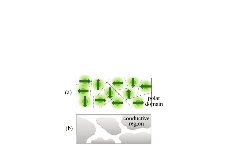
The two models shown Fig. 1, the ferroelectric cluster model (Takesada et al., 2003;
Hasegawa et al., 2003; Katayama et al., 2003) and the conductive-region model (Homes et al.,
2001; Katayama et al., 2003), have been proposed to explain the origin of the giant dielectric
constants. At present, however, it is still not clear which model is better. In the ferroelectric
cluster model, the photo-induced ferroelectric region has a huge dipole moment, where it is
expected that a photo-induced polar domain generates spatial lattice distortion. In the
conductive-region model, on the other hand, the superposition of insulative and photo-
induced conductive regions, which is characterized by the boundaries between the two
regions, makes the apparent dielectric constants to be enormous.
Giant dielectric response has been observed in some types of nonferroelectric materials
(Homes et al., 2001; Wu et al., 2002; Dwivedi et al., 2010). The enormous increase in
dielectric constants is attributed to the formation of barrier layer capacitors and the resultant
Maxwell-Wagner polarization or interfacial polarization. This giant dielectric response often
occurs in materials with grains surrounded by the insulating grain boundary and is
explained by the conductive-region model.
According to the measurement of dielectric constants, a doped crystal Sr
1-x
Ca
x
TiO
3
undergoes a ferroelectric transition above the critical Ca concentration x
c
= 0.0018 (Bednorz
Ferroelectrics – Physical Effects
604
& Muller, 1984; Bianchi et al., 1994). Doped Ca ions are substituted for the Sr ions. The cubic
structure above the structural phase transition temperature (T
C1
) changes into the tetragonal
structure below T
C1
and into the rombohedral structure below the ferroelectric transition
temperature T
C2
. Off-centered impurity ions, which are assumed in the case of impurity
systems such as Li-doped KTiO
3
and Nb-doped KTiO
3
(Vugmeister & Glinchuk, 1990), are
supposed also in the case of Ca-doped SrTiO
3
. Their polarized dipole moments show a
ferroelectric instability below the ferroelectric transition temperature. In the case of Ca-
doped SrTiO
3
, a spontaneous polarization occurs along [110]
directions within the c plane,
where the tetragonal (D
4h
) symmetry is lowered to C
2v
.
Fig. 1. Schematic pictures of (a) ferroelectric cluster model and (b) conductive-region model.
In Ca-doped SrTiO
3
, a UV illumination causes a shift of the ferroelectric phase transition
temperature toward the lower side (Yamada & Tanaka, 2008). The T
C2
reduction under the
UV illumination is considered to be caused by disequilibrium carriers which are captured by
traps and screen the polarization field.
In the present study, we performed three types of experiment in pure and Ca-doped SrTiO
3
;
(i) stationary birefringence measurement in UV light and DC electric fields, (ii) transient
birefringence measurement in UV light and pulsed electric fields, and (iii) transient
absorption and birefringence measurements after the optical pulse excitation using the
pump-probe technique. The photo-induced dynamics of the lattice distortion, the dielectric
polarization, and the relaxed excited state in SrTiO
3
is studied in comparison with the lattice
distortion in the doping-induced ferroelectric phase of Ca-doped SrTiO
3
. We discuss which
model explains the experimental results better.
The experiments are performed on single crystals of pure and Ca-doped SrTiO
3
with the Ca
concentration of x = 0.011. SrTiO
3
was obtained commercially and Ca-doped SrTiO
3
was
grown by the floating zone method. The thickness of the samples is 0.2 mm. The structural
phase-transition temperature, T
C1
=180K, of the Ca-doped SrTiO
3
was obtained from the
temperature dependence of the birefringence (Koyama et al., 2010), and the ferroelectric
phase-transition temperature, T
C2
= 28K, was determined by the measurement of dielectric
constants (Yamada & Tanaka, 2008).
2. Lattice distortion in the UV and DC fields in Ca-doped SrTiO
3
The stationary birefringence is studied to investigate the static properties of the lattice
distortion generated by the UV illumination in comparison with that generated by the
ferroelectric deformation.
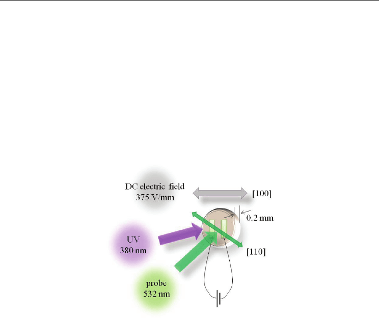
Photo-induced Effect in Quantum Paraelectric
Materials Studied byTransient Birefringence Measurement
605
2.1 Birefringence measurement in the UV light and DC electric fields
The schematic diagram of the birefringence measurement in the UV light and DC electric
fields is shown in Fig. 2. The change in birefringence is detected as the change in the
polarization of a linearly polarized probe light provided by a Nd:YAG laser (532 nm). The
source of UV illumination is provided by the second harmonics (380 nm, 3.3 eV) of the
output from a mode-locked Ti-sapphire laser, whose energy is larger than the optical band
gap of SrTiO
3
(3.2 eV). The intensity of UV illumination is 1.6 mW/mm
2
. Since the repetition
rate of the UV pulses is 80 MHz, this UV illumination can be considered to be continuous in
the present experiment. The UV beam is illuminated on the gap between two Au electrodes.
The electrodes with a gap of 0.8 mm are deposited on a (100) surface of the samples by
spattering. A DC electric field, whose amplitude is 375 V/mm, is applied between the two
electrodes. The DC electric field is applied parallel to [100] direction of the crystal.
Fig. 2. Schematic diagram of the birefringence measurement in the UV light and DC electric
fields.
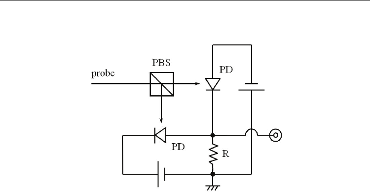
The change in the polarization of the probe light is detected by a polarimeter. The
construction of the polarimeter is shown in Fig. 3. The polarimeter (Kohmoto et al., 2000;
Jones, 1976) detects the rotation of polarization plane of a light beam. A linearly-polarized
beam is split by a polarized beam splitter (PBS) and incident on the two photodiodes (PD)
whose photocurrents are subtracted at a resistor (R). When the polarized beam splitter is
mounted at an angle of 45
o
to the plane of polarization of the light beam, the two
photocurrents cancel. If the plane of polarization rotates, the two currents do not cancel and
the voltage appears at the resistor.
In the present experiment, the birefringence generated by the lattice deformation is detected
as the change in polarization of the probe beam using a quarterwave plate and a
polarimeter. The birefringence generated in the sample changes the linear polarization
before transmission to an elliptical polarization after transmission. The linearly-polarized
probe beam is considered to be a superposition of two circularly-polarized components
which have the opposite polarizations and the same intensities. The generated birefringence
destroys the intensity balance between the two components. The two circularly-polarized
beams are transformed by the quaterwave plate to two linearly-polarized beams whose
polarizations are crossed each other, and the unbalance of circular polarization is
Ferroelectrics – Physical Effects
606
transformed to the unbalance of linear polarization or the rotation of polarization plane.
This rotation is detected by the polarimeter as the signal of the lattice deformation.
Fig. 3. Construction of the polarimeter.
2.2 UV intensity dependence of the birefringence
The ultraviolet intensity dependence of the change in birefringence in Ca-doped SrTiO
3
is
shown in Fig. 4, where the temperature is 6 K and the polarization plane of the probe light is
along the [110] and [100] axes, with which the lattice distortion along the [100] and [110]
axes are detected, respectively. The birefringence increases nonlinearly as the UV intensity is
increased. As is shown in Fig. 4(a), the change in birefringence appears at very weak UV
intensity in the polarization plane only along the [110] axis, rises rapidly, and holds almost a
constant value above 0.5 mW/mm
2
. Figure 4(b), where the horizontal axis is in a logarithmic
scale, indicates that the structural deformation begins at the UV intensity of 10
-3
mW/mm
2
.
The change in birefringence for the probe polarization along the [110] axis is much larger
than that along the [100] axis. These facts imply that the UV illumination causes Ca-doped
SrTiO
3
to undergo a first-order-like structural deformation and generates a lattice distortion
along the [100] axis as a result of the competition between the UV-induced and ferroelectric
deformations, and its threshold value is very small.
Figure 5 schematically shows the direction of the local lattice distortion in pure and Ca-
doped SrTiO
3
. The observed direction of the lattice distortion in Ca-doped SrTiO
3
generated
by the UV illumination is the same as that in the case of pure SrTiO
3
(Nasu, 2003).
2.3 Temperature dependence of the birefringence in the UV and DC fields
We investigated the temperature dependence of the change in birefringence for Ca-doped
SrTiO
3
in the combination of two external fields, UV light (UV) and DC electric (DC) fields.
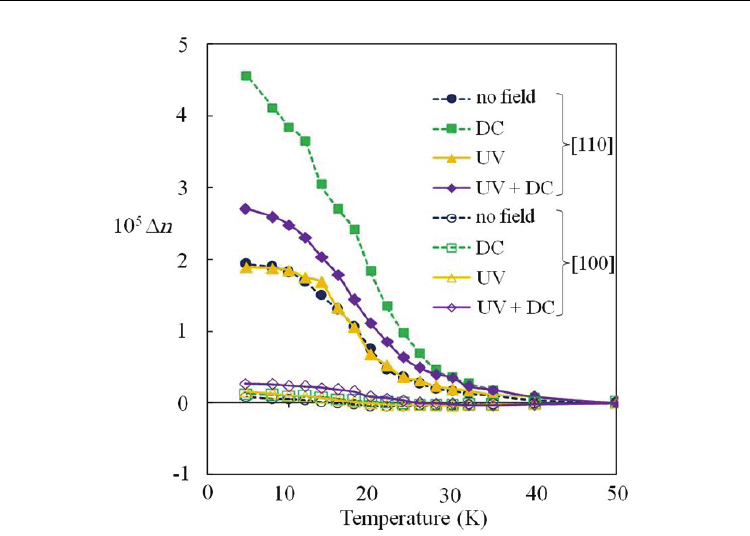
The experimental result is shown in Fig. 6 where the polarization plane of the probe light is
along the [110] and [100] axes. The sample is in the four types of fields; neither UV nor DC
(no field), only DC (DC), only UV (UV), and both UV and DC (UV+DC). The changes in
birefringence for the probe polarization along the [110] axis are much larger than those
along the [100] axis. This means that the optical anisotropy is generated along the [100] axis.
For the probe polarization along the [110] axis without the DC electric field, the change in
birefringence for no field is similar to that for UV, as is seen in Fig. 6, while under the DC
1
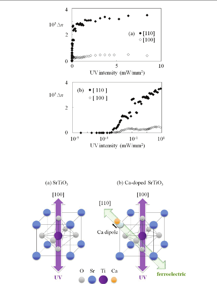
Photo-induced Effect in Quantum Paraelectric
Materials Studied byTransient Birefringence Measurement
607
Fig. 4. UV intensity dependence of the change Δn in birefringence in Ca-doped SrTiO
3
at 6 K,
where the probe-light polarization is along the [110] and [100] axes. The horizontal axis is (a)
in a linear scale and (b) in a logarithmic scale.
Fig. 5. Direction of the local lattice distortion (a) in SrTiO
3
and (b) in Ca-doped SrTiO
3
. The
direction of local lattice distortion generated by the UV illumination is axial along the [100]
axis both for pure and Ca-doped SrTiO
3
. The direction of the local lattice distortion in the
ferroelectric phase of Ca-doped SrTiO
3
is diagonal along the [110] axis.
Ferroelectrics – Physical Effects
608
Fig. 6. Temperature dependence of the change in birefringence for Ca-doped SrTiO
3
in the
combination of two external fields, UV light (UV) and DC electric (DC) fields, where the
polarization plane of the probe light is along the [110] and [100] axes. The sample is in the
four types of fields; neither UV nor DC (no field), only DC (DC), only UV (UV), and both
UV and DC (UV+DC).
electric field the change for DC is different from that for UV+DC. The difference arises from
that of the macroscopic optical anisotropy generated along the [100] axis by the UV
illumination.
In the ferroelectric phase of Ca-doped SrTiO
3
, the direction of the local lattice distortion is
diagonal along the [110] axis (Bednorz & Muller, 1984) as shown in Fig. 5(b). There are six
equivalent diagonal sites where the distortion directions are [110], [1-10], [011], [01-1], [101],
and [10-1]. In no field, it is expected that the six local sites distribute randomly as shown in
Fig. 7(a), and no optical anisotropy is generated. The observed birefringence change Δn
NO
for no field, however, shows that the optical anisotropy grows along the [100] axis at low
temperatures. This may be because that the domain structure due to the structural phase
transition violates the equivalency among the six sites.
In the DC electric field along the [100] axis, on the other hand, the six local diagonal sites in
the ferroelectric phase are not equivalent as shown in Fig. 7(b). The two diagonal sites, [011]
and [01-1] which are perpendicular to the [100] axis, are more unstable in the DC elected
field along the [100] axis than the other four diagonal sites, [110], [1-10], [101], and [10-1].
The random distribution of the four diagonal sites generate a macroscopic optical
anisotropy along the [100] axis. This explains the observed large increase of the
birefringence change Δn
DC
for the [110] probe and small change for the [100] probe.