Lallart M. (ed.) Ferroelectrics - Physical Effects
Подождите немного. Документ загружается.


25
Compositional and Optical Gradient in
Films of PbZr
x
Ti
1-x
O
3
(PZT) Family
Ilze Aulika
*
Center for Space Human Robotics, Italian Institute of Technology - IIT@PoliTO,
Italy
1.
Introduction
Pb(Zr
x
Ti
1-x
)O
3
(PZT) (x = 0-1) films have attracted the attention of researchers for the past 30
years due to their excellent ferroelectric (FE) and electromechanical properties, which have
led to the commercialization of thin PZT films for ferroelectric random access memory
(FeRAM), forming a market of several millions USD annually. Ferroelectricity of perovskite
oxide thin films, especially PZT thin films, can be exploited in semiconductor devices to
achieve non-volatile random access memory (NVRAM) with high-speed access and long
endurance, which can overcome the barriers, encountered in current semiconductor
memory technologies. The ferroelectricity can be also exploited to voltage dependent and
thermally sensitive resistors, gas and humidity sensors. Besides, due to large pyroelectric
coefficient of PZT, it has drawn interest for use in pyroelectric devices (Izyumskaya et al.,
2007; Muralt, 2000; Whatmore et al., 2003).
PZT thin films have remarkable advantages over bulk materials:
• Can be directly deposited on platinized silicon to allow direct integration with
electronics;
• Have superior electromechanical properties compared to other ferroelectric ceramics.
Thanks to that, PZT films have formed an integral part of the microelectromechanical
systems (MEMS) in various applications such as sensors, actuated micromirrors for fine-
tracking high-density optical data storage mechanisms (Yee et al., 2001), and tunable
capacitors for high-frequency microwave applications, microelectromechanical systems,
infrared detectors, applications in optical devices, for instance, rugate filters (Bovard, 1990),
anti-reflection coatings (Oulette et al., 1991), and electro-optic modulators, to name a few.
Low density embedded FE memories are being considered for implementation not only in
commercial devices, such as smart cards and cellular phones, but also for adaptive FE
*
Alexandr Dejneka
2
, Silvana Mergan
3
, Marco Crepaldi
1
, Lubomir Jastrabik
2
, Qi Zhang
4
, Andreja Benčan
5
,
Maria Kosec
5
and Vismants Zauls
6
1
Center for Space Human Robotics, Italian Institute of Technology - IIT@PoliTO, Italy
2
Institute of Physics, Academy of Science, Czech Republic
3
HEARing CRC, University of Melbourn, Australia
4
Cranfield University, School of Applied Sciences, United Kingdom
5
"Jožef Stefan" Institute, Slovenia
6
Institute of Solid State Physics, University of Latvia, Latvia

Ferroelectrics – Physical Effects
580
memories in space applications. FE oxides have demonstrated high resistance to
radioactivity (Philpy et al., 2003; Sternberg et al., 2003), what is important characteristic
for space applications. Radiation test results on a prototype 1 kbit FE memory
demonstrated that FE memory core using FE storage capacitors (Philpy et al., 2003),
combined with hardened-by-design (HBD) CMOS circuitry, can attain high levels of
tolerance to total ionizing dose and single event effects. Preliminary tests indicate that the
hardness of the prototype memory exceeds 2 Mrads total ionizing dose and 163
MeV⋅cm
2
/mg linear energy transfer (LET) latch-up without the need for shielding (Kamp
et al., 2004). FE memory can be designed to compete with any number of traditional
semiconductor memory architectures, including SRAM, SDRAM, EEPROM and Flash
memory (Kamp et al., 2004). This is accomplished by trading off internal write voltage
with retention and endurance and taking advantage of the very fast read/write times of
FE memory. FE memory can be designed to be exactly pin and function compatible with
the other memory types. It follows that the memory types, which much softer to radiation
exposure, can be replaced with FE memory without redesign of the circuit board (Kamp et
al., 2004).
Every application of MEMS requires a different thickness and high quality of the functional
film, leading to the challenge of manufacturing the film of the required thickness, epitaxy
and purity. Among many methods for the fabrication of PZT thin films, chemical solution
deposition (CSD), pulsed laser deposition (PLD), metal organic chemical vapor deposition
(MOCVD), and physical vapor deposition such as RF sputtering have been widely
employed. Among these techniques, chemical solution deposition methods like sol-gel
processing offer low-capital costs, large-scale coating capabilities and easy control of
chemical composition and homogeneity (Izyumskaya et al., 2007). However, the minimum
thickness limitation of around 100 nm per layer for a crack-free and dense film deposited via
CSD requires multiple coatings to reach the final thickness.
The broad applications of PZT films, and inter alia the growing interest in graded refractive
index films for applications in optical devices (Xi et al., 2007; Wang et al., 2001), and
applications in space environment, make it imperative to study the depth profile of
composition and optical properties of thin films throughout a single layer and an entire
coating. Moreover graded PZT thin films, e.g., with amplitude of ±20% at the 53/47
morphotropic phase boundary (MPB), have showed improved electrical performances
(Ledermann et al., 2003), raising importance of depth profile analyses and control.
Wherewith, information on the homogeneity of the films and the physical properties
resulting from different processing methods represents crucial knowledge.
Gradients in optical properties (refractive index n, extinction coefficient k, abortion
coefficient
α
, band gap etc) and chemical composition gradients have been reported, e.g., for
sputtered PZT films (Deineka et al., 1999 and 2001; Vidyarthi et al., 2007; Chang et al., 2005)
and for CSD-fabricated PZT films (Aulika et al., 2009; Calamea and Muralt, 2007; Etin et al.,
2006; Impey et al., 1998; Ledermann et al., 2003; Marcus and Schwartz, 2000; Watts et al.,
2005). Variation of chemical composition throughout the film thickness due to
inhomogeneity results in variation of physical properties such as optical properties of the
films, resistance to irradiation, and lowers or improves the performance of
electromechanical systems. The understanding of the compositional gradient and physical
properties resulting from different processing methods is crucial. Thus, the knowledge of
the optical gradient within a film allows identification and further optimization of the thin
film performance and applications in piezo- and ferro-devices.

Compositional and Optical Gradient in Films of PbZr
x
Ti
1-x
O
3
(PZT) Family
581
2. Depth profile detection methods
A challenging aspect of homogeneity studies lies in the development of an appropriate
characterization method, since the compositional variation must be determined on a small
scale, within 100 nm. Depth profile detection methods can be divided into two categories:
• Destructive,
• Non-destructive methods.
The 1
st
category typically allows local visualization of thin films and element concentration
analyses, what requires etching or cross section of the sample accompanied with
spectroscopy methods. For visualization of the films well established microscopy techniques
such as scanning electron microscopy (SEM), transmission electron microscopy (TEM), and
atomic force microcopy (AFM) are widely used in the practice. For compositional analyses
(qualitative and quantitative) energy-dispersive x-ray spectroscopy (EDXS, known also as
EDX or EDS), photoelectron spectroscopy (XPS), secondary ion mass spectrometry (SIMS),
Rutherford back scattering (RBS), electron energy loss spectroscopy (EELS) and other
spectroscopies are applied. For example, the approach can be thought of simply as the
analytical implementation of rf-sputter etching, where the atomized material is analyzed by
its characteristic optical emission. This method is known as radiofrequency glow discharge
atomic emission spectroscopy (rf-GD-AES) (Marcus and Schwartz, 2000): permits the depth-
resolved elemental analysis of metallic, semiconducting, and insulating materials over
depths of 20 nm–150 μm in a rapid fashion < 0.1–5 μm/min. The analytical data are reported
as elemental emission intensities as a function of sputtering time, termed a qualitative depth
profile. Qualitative depth profile can be also analyzed by the detection of concentration
gradients of the chemical elements of PZT thin films using Z contrast TEM with EDX
(Ledermann et al., 2003). In the work of Watts et al., 2005, the EDX was performed on
PbZr
0.52
Ti
0.48
O
3
(PZT 52/48) thin films. Compositional profiles were determined along with
analysis of the state of oxidation of the lead. The data were compared with bulk
polycrystalline material as standard giving quantitative depth profile of the films.
Similar method to rf-GD-AES was presented in the work of Vidyarthi et al., 2007, where
chemical composition and depth profiling of PZT films was investigated by glow discharge
optical emission spectroscopy (GDOES). They used two samples, which chemical
composition was measured by RBS, to calibrate GDOES for PZT quantitative compositional
analysis.
SIMS was used to monitor the Pb, Zr, Ti, and C secondary ions in addition with the EDX to
determine the oxidation state of the elements (Etin et al., 2006). Pb4f, Zr3d, and Ti2p and O1s
spectra were used for calculation of film composition as a function of depth using
calibration equations (Sugiyama et al., 2003 and 2004) presenting quantitative depth profile
analyses.
Fascinating work have been done by Parish et al., 2008, where the use of multivariate
statistical analysis (MSA) of EDS spectrum images (SIs) in scanning TEM (STEM) was
extended to allow the two-dimensional (2D) quantitative analysis of cation segregation and
depletion in PLZT thin films. STEM-EDS SIs method allows high-resolution (≤ 10 nm)
quantification of cation distributions. Zr/Ti and La segregation are found to develop in a
decidedly nonplanar fashion during crystallization, highlighting the need for 2D analysis.
The drawback for TEM and STEM-EDS SIs investigations is tedious and time-consuming
sample preparation. Investigation using other methods such as RBS results in sample
modification or even destruction after analysis. Also all other methods mentioned before

Ferroelectrics – Physical Effects
582
goes hand to hand with either sample distraction, compositional modification (e.g.,
impregnation of ions during milling with ion beam) or specific sample preparation needs.
To conclude, examples given above for depth profile detection suffer from being ‘‘local’’,
intrusive, destructive and unsuitable for real-time, inline monitoring of processes and
surface/interface modifications of thin films.
What about the 2
nd
category: non-destructive methods of depth profile detection? In this
category only sensitive, accurate, contactless optical techniques are giving this opportunity
to analyze thin films in non-destructive way. Well know optical methods are, for example,
reflectometry, interferometry and spectroscopic ellipsometry (SE). SE have several
advantages regarding other optical methods eliminating such disadvantages as dependence
on the intensity of the light source (reflectometry), vibrations and atmospheric disturbances
(interferometry). SE is nondestructive, nonintrusive, and noninvasive, contactless optical
technique, applied not only for the optical characterization of bulk materials and thin films,
but also for in situ real-time measurement of multilayered film structures, interfaces,
surfaces, and composites, during fabrication and processing.
SE has long been recognized as a powerful method for the characterization of thin films and
their inhomogeneity. It has already been applied to refractive index depth profile studies of
oxynitride SiO
2
N
x
films (Callard et al., 1998; Nguyen et al., 1996; Snyder et al., 1992; Rivory,
1998;) (additionally confirmed by chemical etching (Callard et al., 1998)), lead silicate glass
(Trolier-McKinstry and Koh, 1998), oxidized copper layers (Nishizawa et al., 2004),
polymers (Guenther et al., 2002), semiconductor indium tin oxide (ITO) films (Losurdo,
2004; Morton et al., 2002), sol-gel PZT thin films (Aulika et al, 2009) confirmed by TEM and
EDX, and RF-sputtered self-polarized PZT thin films (Deineka et al., 2001), and was
confirmed by discharge optical emission spectroscopy (GD-OES) and pyroelectric profile
measurements by the laser intensity-modulation method (LIMM) (Deineka et al, January,
2001; Suchaneck et al., 2002). SE has also been applied to the study of ion implantation depth
profiles in silicon wafers and confirmed by RBS (Boher et al., 1996; Fried et al, 2004). The
sensitivity of SE was demonstrated on graded oxygen compositions in YBa
2
Cu
3
O
7-
δ
(YBCO)
thin films, in which it was able to detect changes in the oxygen concentration to within one
unit cell (Gibbons, and Trolier-McKinstry, 1999).
SE cannot quantitatively examine cation distribution at a length scale comparable with the
feature sizes like in a case of STEM-EDS SIs method (Parish et al., 2008) since the measured
area depends on the diameter of the incident light spot of SE (typically ~ 3 mm, by using
focusing nuzzles it can be reduced till ~ 0.1 mm). As the result it is easy to perform relatively
large area scans of the sample using SE, and evaluate information (for example, depth
profile) in average across many features simultaneously. And thus SE studies gives an
opportunity in non-destructive, rather fast and easy way to analyze the inhomogeneity of
material and helps to understand how processing affects structure and thus properties in
this system. Now more in details about this method.
2.1 Spectroscopic ellipsometry
Not very long time ago the development of spectroscopic ellipsometry made it possible to
investigate the complex refractive index of thin films and bulks in a wide spectral range
(gives access to fundamental physical parameters; morphology, crystal quality, chemical
composition, or electrical conductivity), and detecting inhomogeneities of thin films,
eliminating such disadvantages of other non-destructive and contactless optical technique as

Compositional and Optical Gradient in Films of PbZr
x
Ti
1-x
O
3
(PZT) Family
583
dependence on the intensity of the light source (reflectometry), vibrations and atmospheric
disturbances (interferometry) (Tompkins and Irene, NY 2005).
Typical ellipsometers can accurately measure ψ and Δ better than 0.01°. Due to such a high
accuracy a change of the refractive index of 10
-3
– 10
-4
, and film thickness changes down to
the sub-Å scale can easily be resolved with this technique (Tompkins and Irene, NY 2005). A
reflectometer system can not accurately measure intensity values better than 0.1%, and
therefore a reflectivity measurement is not sensitive enough for small changes of the
material`s optical properties and for thin film thicknesses.
With spectral ellipsometry one can measure the dispersion of the complex dielectric
constant of bulk materials and thin films with very high accuracy. This technique does not
require a large size of the sample; it is enough to have a size of ~ 5×5 mm. In situ spectral
ellipsometry studies allow detecting phase transition in thin films and surfaces (Dejneka et
al., 2009), as well as of the interface what is very important for thin film and crystal studies.
For advanced optoelectronics and bandgap engineering applications is important to
investigate the relationship between the microstructure, sample preparation conditions &
optical properties. SE gives opportunity to detect technologically and scientifically
important properties of thin films such as optical bang gap (Dejneka et al., 2010), thermo-
optical properties (Aulika et al., 2007 and 2009; Dejneka et al., 2009), and optical gradient
(Aulika et al., 2008 and 2009; Deineka et al., January, 2001).
2.2 What ellipsometry measures?
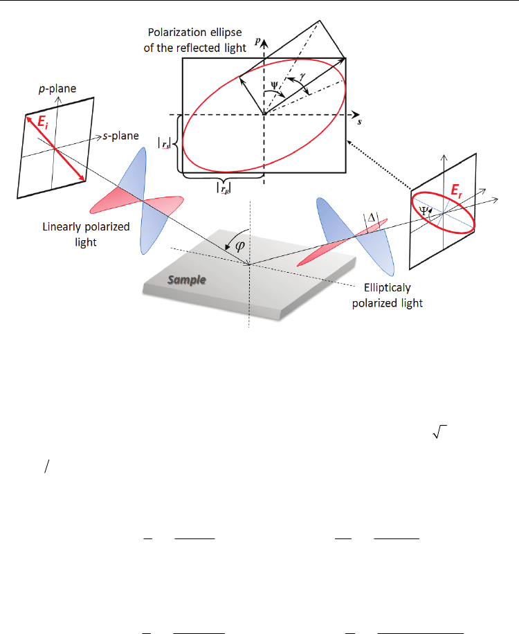
Ellipsometry measures the change of the polarization state of light upon reflection. It
overcomes two major problems of conventional spectroscopy or reflectivity: the phase
problem (in ellipsometry the phase is measured and does not have to be calculated by
Kramers-Kronig relation) and the reference problem (ellipsometry requires relative, not
absolute, intensities). Paul Drude was the first to study optical properties using the
ellipsometry technique. He published the equation of ellipsometry in 1887, and his
experimental results in 1888. Generally, after reflection on a sample the polarization state of
the light is elliptical (Fig. 1). The electrical field components parallel and perpendicular, E
ip
and E
is
, with respect to the plane of incidence change their amplitude and phases due to
reflection upon the sample. These total reflective coefficients are connected with the main
ellipsometric angles ψ and Δ (Tompkins and Irene, NY 2005)
tan
p
s
r
r
ψ=
and
pip
i
sis
rE
tg e
rE
Δ
ψ
===γ,
where
γ
is the quantity of ellipticity, and Δ = δ
p
− δ
s
is the phase shift of the p and s-polarized
light (Fig. 1). Reflection and transmittance coefficients can be found from Fresnel formulas,
which on the other hand are containing information about the optical constants, thickness of
the thin film (or thin films in the case of multilayer) incident angle of the light, and phase
suspension of the light.
ψ = ψ (ε, σ, ω), and Δ = Δ (ε, σ, ω), where ε is the real part of dielectric function, σ is the real
part of conductivity, and ω is the frequency. There are two equivalent descriptions: the first
one operates with real and imaginary parts of the dielectric function ε
1
, ε
2
, the second one
operates with the real part of the dielectric function and the real part of the conductivity.
The ratio between conductivity and dielectric function σ ∝ ıωε makes these descriptions
equivalent.
Ferroelectrics – Physical Effects
584
Fig. 1. Light reflecting from a sample at angle
ϕ
. The linearly polarized incident light has
two electric field components E
ip
and E
is
in the directions parallel and perpendicular to the
propagation plane, respectively. The reflected light has elliptical polarization.
The main ellipsometric angles ψ and Δ are the functions of dielectric constants of the sample:
Consider the complex refractive index as nnik
=
−
, where n – refractive index, k – extinction
coefficient, it can be written in a form of dielectric permittivity
(1 )nn i
=
−α= ε
(Born, and
Wolf, Cambridge University, 1999), where
12
i
ε
=ε − ε - complex dielectric permittivity, and
4 kα= π λ
- absorption coefficient. First, the dielectric permittivity is a response function,
therefore
(
)
(
)
∗
ε−ω=ε ω. Second, from the causality principle we have the Kramers-Kronig
(KK) relations (Tompkins and Irene, NY 2005)
2
1
22
0
2()
() 1
xx
Pdx
x
+∞
ε
εω−=
π
−ω
∫
and
1
2
22
0
2()1
()
x
Pdx
x
+∞
ωε−
εω=−
π
−ω
∫
,
where P – is the symbol of the main quantity of the integral. For isotropic media
2
()n =εω
,
22
1
()nk−=εω,
2
2()nk
=
εω, then KK can be written in
22
22
0
4()()
() () 1
xn x k x
nk P dx
x
+∞
ω− ω− =
π
−ω
∫
and
22
22
0
() () 1
()()
nx kx
nk P dx
x
+∞
ω−−
ωω=
π
−ω
∫
.
The combination of KK relations with physical arguments about the behavior of optical
conducts us to the sum-rule expression.
Optical properties of materials can be modeled also by considering the field re-radiated by
the induced dipoles of the classical oscillators. Such classical oscillators are Lorentz
oscillator, for example. In this model the dipole radiation field interferes with the incident

Compositional and Optical Gradient in Films of PbZr
x
Ti
1-x
O
3
(PZT) Family
585
field in such a way as to produce absorption or refraction. The Lorentz model assumed that
an electron bound with the nucleus as a harmonic oscillator. By solving the equation of
motions, distribution of the complex dielectric function can be found as
ε
(Tompkins and
Irene, NY 2005)
()
()
2
2
1
c
A
EEEiB
∞
⎛⎞
⎜⎟
ε=ε +
⎜⎟
−−
⎝⎠
.
The model fitting parameters
ε
∞
, E
c
,, E, B and A are in units of energy, and they are
respectively: the high-frequency lattice dielectric constant, the centre energy of the oscillator,
the photon energy, the vibration frequency (broadening) of the oscillator, and the amplitude
(strength) of the oscillator.
Unfortunately the Lorentz oscillator (LO) does not fit well the characteristics of the complex
dielectric function at the near ultraviolet and ultraviolet (UV) regions for ferroelectrics and
some semiconductors (Bungay and Tiwald, 2004; Jellison et al., 1997; Synowicki and Tiwald,
2004). LO functions were used to model molecular or lattice vibrations in the infrared
(Bungay and Tiwald, 2004), complex refractive index of conductive oxides (Synowicki,
1998), metals (Brevnov and Bungay, 2005), and ferroelectrics till the absorption edge
(Lappalainen et al., 2005). LO is symmetric in shape, and the high and low energy sides of
the function decrease at the same rate. It is because the low energy portions of the
ε
’ curves
are most strongly affected by the area under of the curve (area is proportional to A⋅B), and
the peak shifts to lower energies as broadening increases. As a result LO have long
asymptotic tails away from the absorption peaks and can cause unacceptable absorption
artifacts in transparent regions.
Tauc-Lorentz (Jellison and Modine, 1996) and Cody-Lorentz oscillator (TLO and CLO) are
more flexible functions at the fundamental band gap E
g
and higher energies in the UV, since
these functions rapidly decrease to zero away from their center energy and do not have long
asymptotic tails as LO which can result in unwanted absorption through the band gap and
below. As the result the typical absorption of dielectrics due to the electrons transition from
the valence band to the conductive band at high photon energies can be very well described.
Depending on the material under the studies the most suitable oscillator hast to be chosen
for modeling its complex dielectric function.
2.3 Modeling of depth profile
For thin films the most interesting anomalies of the properties are related to their spatial
nonuniformity. The details of this nonuniformity depend on the conditions on the film
surfaces (substrates, electrodes). The most important characteristic of ferroelectric thin film
is their
nonuniform polarization. Its calculation can be performed on the base of
phenomenological theory with polarization gradient in free energy density (Deineka et al.,
2001; Glinchuk et al., 2000; Tilley, Gordon and Breach, Amsterdam, 1996; Wang et al., 1995;,
2002).
It was found (Glinchuk et al., 2000) that dielectric susceptibility is also
inhomogeneous and it can be calculated, for example, on the base of Lame equation. As a
matter of the fact obtained polarization P(z) profile is related to that of optical refraction
index: 1/n
2
~ (1/n
0
2
)
(1 + P(z)
2
). Due to the proportionality of the refractive index to the
square of the spontaneous polarization, the inhomogeneity of the film can be detected as a
refractive index depth profile.
Ferroelectrics – Physical Effects
586
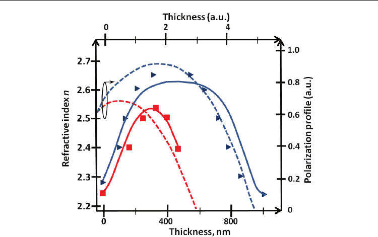
Fig. 2. Comparison the theoretically calculated (solid lines) and experimentally determined
(symbols) refractive index depth profiles for PZT films of different thickness, and
polarization profiles (discontinuous line) for the films with different thickness (Deineka et
al., 2001).
Theoretically calculated and experimentally obtained optical profile for
perovskite/pyrochlore double layer stacks of PZT (deposited using sputtering on platinized
silicon wafers by Siemens AG, Munich (Germany) are presented in Fig. 2. According to
theoretical prediction (Glinchuk et al., 2000),
the behavior of polarization profile changes
considerable for very thin PZT
films. This is illustrated in Fig. 2b: the film polarization
decreases monotonous with the thickness.
Polarization profile in ferroelectric thin films can be caused, e.g., during deposition, by
chemical element distribution, by strains etc , and “reflected” in other physical properties of
the film, for example, the refractive index profile. It should be noticed that any change in the
sample structure will affect the polarization and optical properties of the material,
irrespective of whether it is a result of the stoichiometry, compositional gradient, internal
stresses, etc. Using spectroscopic ellipsometry it can be detected and modeled.
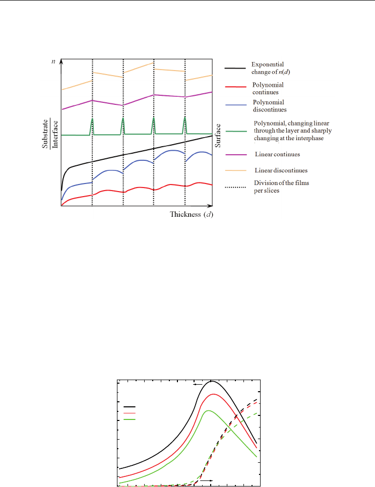
The depth profile of the optical properties is modeled by dividing the single layer by slices,
and the shape of the grading profile is characterized using:
•
Simple graded model, e.g., exponential variation of the refractive index n versus film
thickness (n ~ ab
d
);
•
Function based graded model, e.g., polynomial (n ~ A
0
+ A
1
d + A
2
d
2
+ …).
Some examples of the depth profile of n are represented in Fig.3.
If the film has no gradient of the refractive index, there is no change of n, and in case of the
simple graded model, exponent is equal to 1. Variation of the refractive index from the
substrate to the film surface is adjusted by exponent greater or smaller then 1. In this graded
model the fitting parameters are value of exponent and variation of n. Optical gradient
Compositional and Optical Gradient in Films of PbZr
x
Ti
1-x
O
3
(PZT) Family
587
typically is calculated in the wavelength region of 500 – 1000 nm, where ferroelectrics and
dielectrics are not absorbing the light, to minimize fitting parameters correlation caused
artifacts.
Fig. 3. The optical depth model examples applied to fit experimental SE data: exponential
variation of n trough the film, considering it as a one complete layer; discontinues liens -
exponential variation of n at the each layer of the film. The different shapes of exponent
were accomplished by changing the value of exponent and variation of the refractive index.
3. Optical gradient in PZT
3.1 Optical properties of PZT films
In the Fig. 4 refractive index n and extinction coefficient k as a function of photon energy for
PZT thin films with different composition are presented. These are typical dispersions of
optical constant for PZT thin films with no compositional gradient. With increase of Zr/Ti
ratio refractive index decreases, while optical band gap is practically not changing, suggesting
that the substitution of Ti by Zr does not change much the electronic band structure of PZT.
1.52.02.53.03.54.04.55.05.5
2.4
2.6
2.8
3.0
3.2
3.4
0.0
0.4
0.8
1.2
1.6
k
n
E (eV)
PZT on Pt
With major (111) orientation
Thickness 70 - 95 nm
PZT 30/70
PZT 52/48
PZT 95/05
Fig. 4. Refractive index n and extinction coefficient k of sol-gel PZT thin films of 3 different
compositions. Complex dielectric function of the PZT was evaluated by fitting experimental
data of spectroscopic ellipsometry. n and k was modeled using Tauc-Lorentz oscillator.
Ferroelectrics – Physical Effects
588
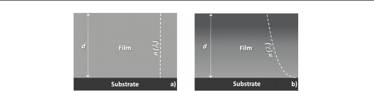
Fig. 5. Schematic illustration of the film with thickness d with a) no change of refractive
index n and b) with change of n at wavelength
λ
i
from the bottom to the top of the film
presenting optical gradient in the film. Change of n with d can have different nature (see Fig.
2), depending on the chemical/physical processes involved.
The most sensitive parameter to the composition change in PZT is refractive index, and
compositional gradient can be detected as an optical gradient (e.g., refractive index change
in the depth of the film). Film with no compositional gradient has no change of n and k
within the film with the thickness d, while films with compositional gradient will have
depth profile of optical constants as schematically presented in Fig. 5.
3.2 Factors inducing the gradient
Structural and ferroelectric properties, growth rate, phase composition, and stoichiometry of
PZT films depend on a number of film deposition parameters, among which are:
•
Chemical solution deposition (CSD) or sol-gel technique: precursor solution (lead
content of the starting solution; thermal decomposition of raw components), a low-
temperature heat treatment at 300-400°C (pyrolysis) to remove organic components,
high-temperature annealing (600-700°C) to form a dense crystalline layer, substrate
(difference in thermal expansion coefficient between the film and the bottom electrode),
annealing atmosphere; how annealing was accomplished (furnace, hot plate, rapid
thermal annealing etc)
•
Hydrothermal method: Gas pressures, synthesis temperature;
•
Sputtering: substrate temperature, gas pressure and composition, sputter power,
target-to-substrate distance, and target composition;
•
Pulsed Laser Deposition (PLD): laser parameters (laser spot size, fluence, wavelength,
repetition rate, power), properties of the target material, ambient gas pressure and
composition, substrate type and temperature, substrate-to-target distance and target-
substrate geometry;
•
Metal-Organic Chemical Vapor Deposition (MOCVD): substrate temperature,
chamber pressure, and oxygen partial pressure.
The gradient (either compositional and/or optical) can be induced by following factors (see
Fig. 6):
•
Thermodynamically driven diffusion and/or kinetic demixing (Cabrera, and Mott,
1948; Impey et al., 1998; Ohba et al., 1994; Okamura et al., 1999; Wagner, 1971; Watts et
al., 2001 and 2005);
•
Stress (e.g., lattice mismatch and misfit stress with the substrate; stress dependence of
film thickness), (Corkovic et al., 2008; Izyumskaya et al., 2007; Gkotsis et al., 2007);
•
Nucleation processes (Izyumskaya et al., 2007; Ohba et al., 1994; Okamura et al., 1999).
Depending on deposition processes involved, some or even all of these factors can be
incorporated and accountable for gradient formation in the films. For the same film