Hoque. Advanced Applications of Rapid Prototyping Technology in Modern Engineering
Подождите немного. Документ загружается.

A Wafer-Scale Rapid Electronic Systems Prototyping Platform
211
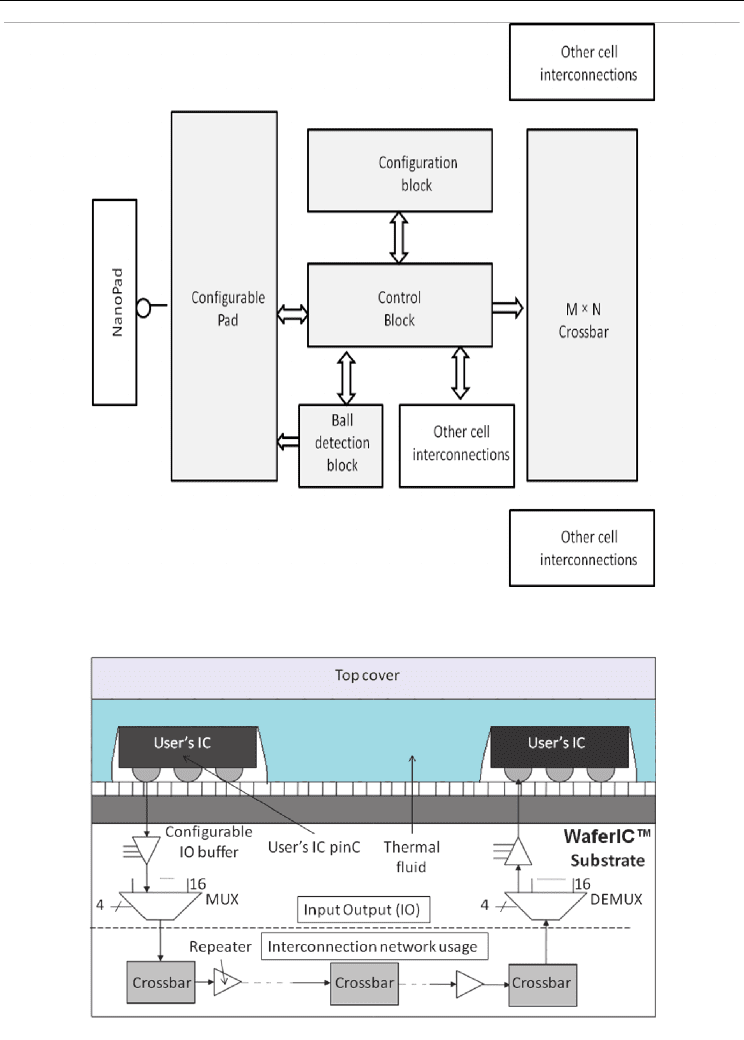
Fig. 4. Architecture of a Unit-Cell.
Fig. 5. Overview of an interconnect chain embedded in the WaferIC.
Advanced Applications of Rapid Prototyping Technology in Modern Engineering
212
NanoPad to another. Figure 5 presents an example of one possible route through the
interconnect chain. The interconnect chain is made of three main elements. The first element
is the input/output (IO). It is made of configurable IO buffers set up at each NanoPad,
which allow the WaferIC to supply a variety of voltage levels in order to support different
types of uICs. To maintain signal integrity, an interconnect chain is implemented with the
second element, a set of repeaters inserted at regular interval. The third element is the
crossbar, used to route the signal in different directions as needed in the WaferNet. More
details about the crossbar architecture are given in section 2.3.
2.3 WaferNet, a defect tolerant interconnection network
The WaferNet was designed to support most standard uICs, including processors, FPGAs,
and memories regardless of the packages’ pin-count and density. The large interconnect
density offered by the multiple metal layers available in mature CMOS technologies enables
the WaferNet to support point-to-point, point-to-multipoint and busses. The WaferNet is a
scalable multi-dimensional mesh network, which can route a large number of connections
without conflict as required by dense PCBs.
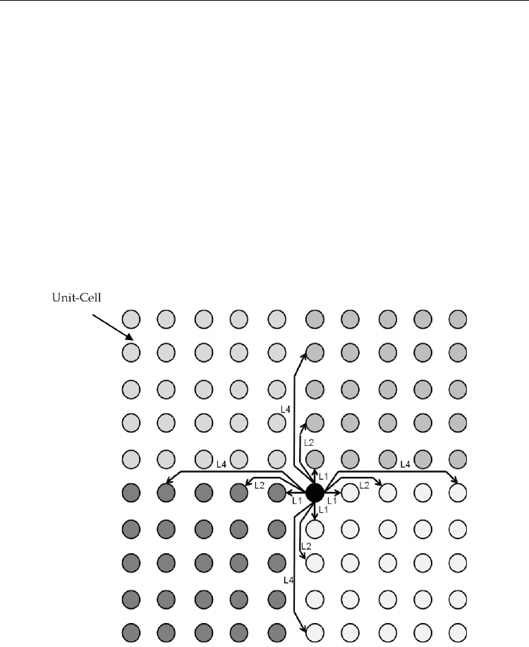
Fig. 6. Example of interconnections with other cells for the Unit-Cell colored in black where
L stands for the length of links measured as a distance in Unit-Cells.
Contacts between adjacent interconnections can be achieved using a two dimensional
neighbor-to-neighbor mesh, but this approach becomes inefficient in the case of distant
interconnections. Thus, in WaferNet, each network node is linked to K others in each
physical direction (N-S-E-W). Figure 6 shows the progressive increase in length of K links in
A Wafer-Scale Rapid Electronic Systems Prototyping Platform
213
a given direction. Indeed, the length of links grows according to a geometric series. As
depicted in figure 6, each node follows the same pattern of connection; when K=3, for
example, the node depicted in black is connected to the 1st, 2nd and 4th neighboring nodes
in each direction (N-S-E-W). The value of K is a key design parameter that influences
complexity, interconnect density and defect tolerance. Indeed, increasing K contributes to
improve defect tolerance as each crossbar supports more links than the minimum required.
Moreover a dense NanoPad array in which each component ball intersects a plurality of
NanoPads contributes to defect tolerance.
The WaferNet has a regular architecture based on a Unit-Cell elementary tile in order to
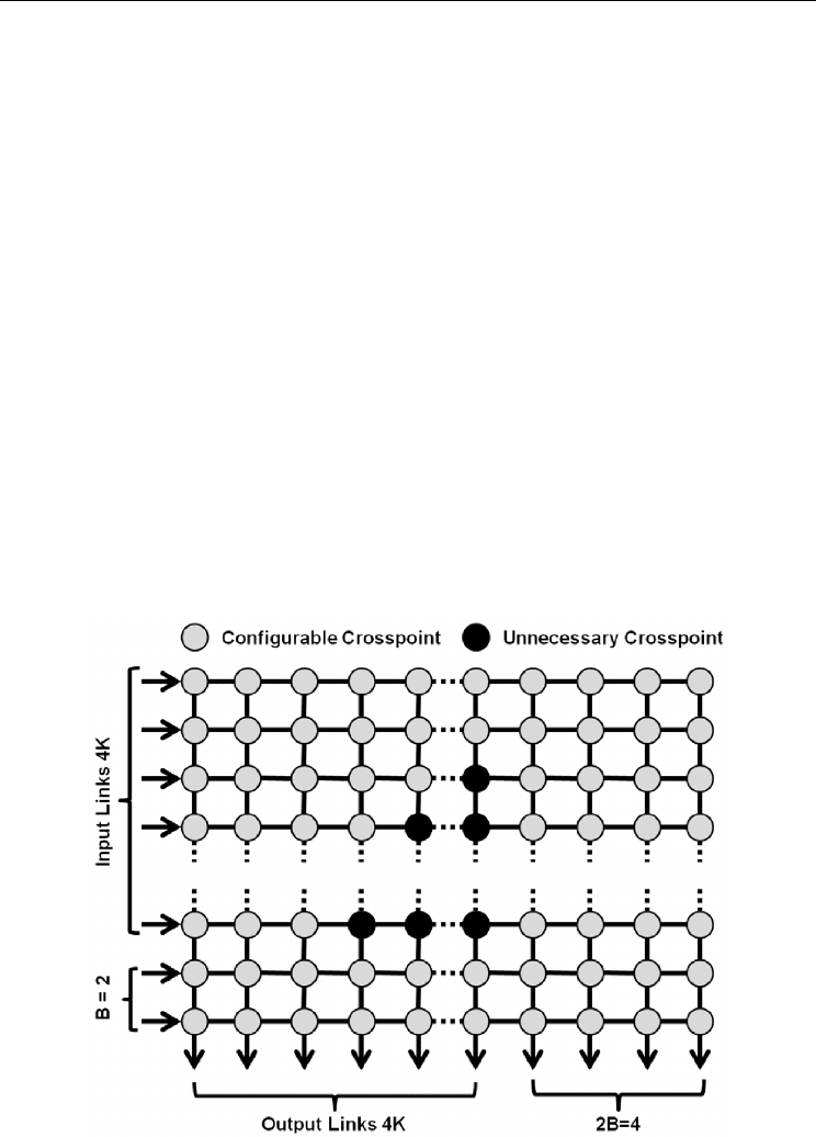
meet the wafer-scale integration constraints. The N×M crossbar that is part of each cell can
route its 4×K (4 directions) inward signals to its 4×K outward signals. Each Unit-Cell is
designed to handle up to B uIC balls. A regular uIC ball implies one or more crossbar input
or output. By contrast, each bi-directional uIC ball consumes two crossbar outputs. One of
them is used to control the signal direction. The size of the crossbar (NM) is therefore
related to the number of uIC balls supported by a cell and its neighbor (as needed to
support defect tolerance), where N 4×K+B and M 4×K+2B. In general, increasing M or N
makes the network more robust to faults or defects.
2.4 Crossbar implementations
The crossbar required by the network architecture utilizes a large part of the Unit-Cell logic.
To illustrate that complexity, the internal architecture of a crossbar for a given variable K,
B=2 is shown in figure 7. Three approaches were considered for crossbar implementation:
(1) crosspoint-based crossbar, (2) tri-state based crossbar, and (3) switch-based crossbar. All
Fig. 7. Crossbar implementation using crosspoints.
Advanced Applications of Rapid Prototyping Technology in Modern Engineering
214
three techniques were implemented at the circuit level and these implementations were
compared in order to find the best solution for the WaferNet.
The first solution implements crossbars with crosspoints. This crosspoint-based crossbar
(Fig. 7) uses a single memory element per crosspoint that is responsible for propagating or
not propagating some signals to any given column. In figure 7, several crosspoints are
labeled as unnecessary from a functional standpoint. However, some implementations may
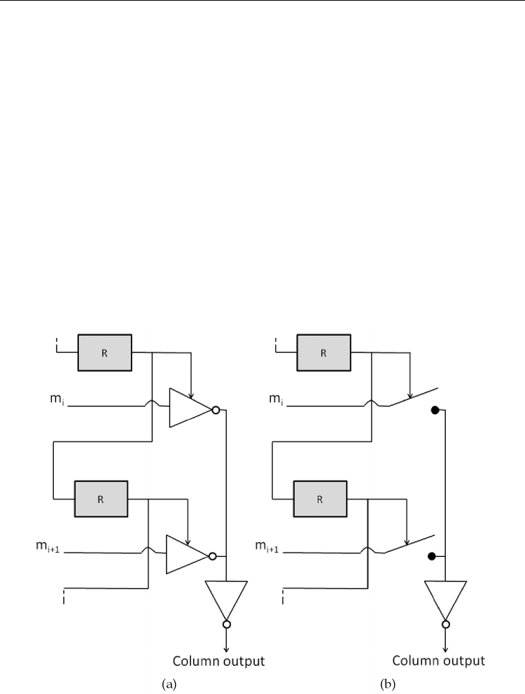
keep these crosspoints for layout regularity. Another solution is to use pass-transistor
switches. Such switches (see Fig. 8 (b)) are notably used to implement FPGA crosspoints.
While pass transistor switches are bi-directional, their implementation requires special care
due to the threshold voltage losses they induce. A solution to alleviate threshold voltage
losses is to use transmission gate switches at the cost of more silicon area and parasitic
capacitances. The advantage of using pass transistors or transmission gates to implement
switch based-crosspoints may be offset by the relatively large resistivity that accumulates as
a signal passes through several layers of switches. A common means to combat this effect is
to regenerate the signals by inserting buffers at regular intervals. To avoid unintentional
shorts on column lines, the crosspoints and their related configuration sequence must be
carefully designed. Shorts could generate high peak currents that would stress the
components. This could reduce significantly the reliability and product life of the
WaferBoard, and increase its power consumption.
Fig. 8. Examples of crossbar implementations (a) Tri-state based crosspoints, (b) switch-
based crosspoints.
A Wafer-Scale Rapid Electronic Systems Prototyping Platform
215
Another approach for implementing crossbars is to use multiplexers. To implement a full
N×M crossbar, M N-input multiplexers (one per column) are needed. A total of N log
2
M
configuration memory elements are required while log
2
M memory elements are required for
each column multiplexer. An advantage of using multiplexers to implement the crossbar is
the manner in which short-circuits are prevented compared to crosspoint-based crossbars.
Moreover, the number of memory elements, especially for large K, is considerably reduced
with this approach.
Several crossbars were designed according to these various styles for K=7, and the resulting
implementations were compared. Table 1 summarizes the logic area extracted from RTL
synthesis for four implementations. Some results are also reported for partial pruned
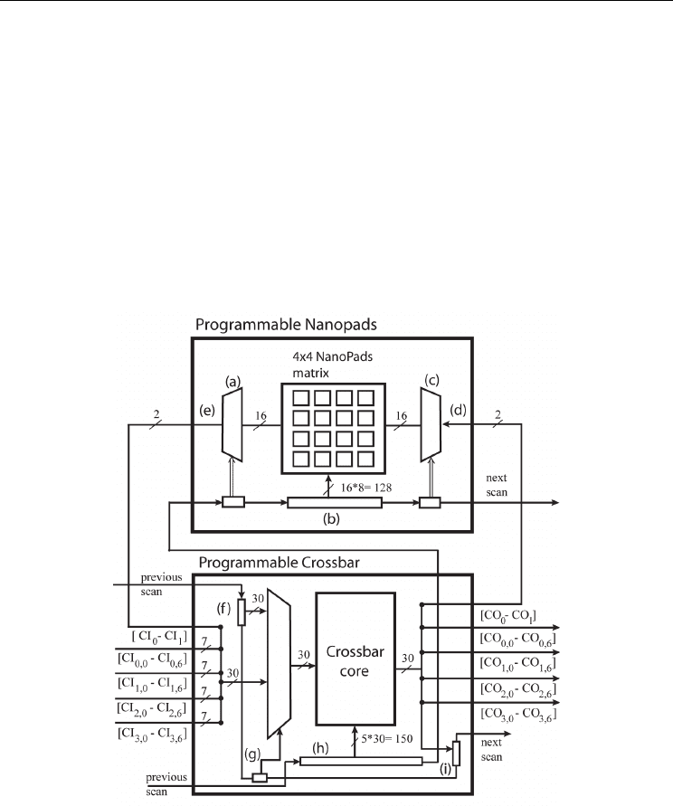
crossbars (see figure 7). In figure 9 that shows internal details of a cell , the incoming links in
the N-E-S-W physical directions are called CI0,[0..6], CI1,[0..6], CI2,[0..6], and CI3,[0..6]
respectively.
Fig. 9. Unit-Cell structure with its two internal scan chains : configuration scan ((h) and (b)),
test and diagnosis scan ((f), (g) and (i)). (Basile-Bellavance, Blaquière & Savaria, 2009).
Our results, reported in Table 1, demonstrate that the multiplexer based crossbar occupies
less area than the tri-state based crossbar. This is due to the fact that the crossbar complexity
grows as O(N log
2
M), where N is the number of inputs and M is the number of outputs. This
is to be compared with a linear growth O(N×M) in total area with crosspoint–based
crossbars.
Advanced Applications of Rapid Prototyping Technology in Modern Engineering
216
Crossbar type Total area (µm
2
) Memory area (µm
2
)
Memory proportion
(%)
Full Tri-state based 125400 54240 43.3
Partial tri-state based
91521 41764 45.6
Full mux based 45050 9040 20.2
Partial mux based 43538 9040 20.8
Table 1. Synthesis results of crossbar implementations for K=7.
Based on these results, the first full wafer prototype that was produced use K=6 to fully take
advantage of the interconnect density that multi-metal-layer lithography provides with the
adopted standard 0.18 µm CMOS process (logic and interconnect complexities were too high
to fit in the available area when K=7). Thus the implemented crossbar includes 6 incoming
6 links and outgoing links in each direction (Fig. 9). The Unit-Cell includes also internal scan
chains that are used to configure the crossbar and to get access to crossbar I/Os using a
protocol similar to that found in the IEEE standard 1149.1 (referred as JTAG here) (Parker,
1998). The Unit-Cell internal scan chains can be daisy chained and accessed through the
standard four JTAG ports, one set per reticle image (TDI, TDO, TCK and TMS).
2.5 WaferBoard power distribution
The first implemented WaferIC has 4,864 regularly distributed Through Silicon Vias (TSVs).
The TSV technology (Motoyoshi, 2009; Rimskog, 2008) is a mature technology that allows
integration of 3D IC or 3D packaging (Papanikolaou, 2011; Lau, 2009; Mitsumasa, 2009).
Power and ground must be distributed to uICs through these TSVs with embedded
programmable regulators within the NanoPads to ensure proper power supply integrity.
Effectively, decoupling capacitors cannot be placed on the top side of the WaferIC and
integration of sufficient capacitance is impossible due to silicon area constraints imposed by
the WaferIC. Consequently, the chosen architecture needs to rapidly deliver a regulated
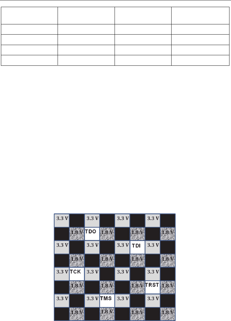
Fig. 10. TSV distribution over the reticle image.
A Wafer-Scale Rapid Electronic Systems Prototyping Platform
217
voltage without the benefit of adding capacitors. The voltage regulator in each NanoPad is
designed to provide a range of standard VDD levels such as 1.0, 1.5, 1.8, 2 and 2.5 V. Each
reticle image has an array of 8×8 TSVs as depicted in Figure 10, which are used to supply
ground (27 TSVs), and two levels of power 1.8 V and 3.3 V (16 TSVs each). A set of 5 TSVs is
reserved for JTAG signals to configure the device. Each NanoPad can deliver up to 100 mA
to a uIC ball load. The power delivered to the wafer through TSVs comes from an array of
independent power sources that can supply 15 A each, and a total of 315 A to the WaferIC.
The WaferIC is made of analog and digital parts. The analog part comprises I/O buffers, one
per NanoPad, and distributed power regulators, responsible to supply power to uICs. The
digital portion consists of the embedded programmable interconnect network and of the
defect tolerant scan chains used for configuration purposes.
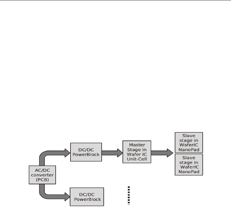
Figure 11 presents the WaferIC power-supply tree structure with a single power-source at
its root and a distributed set of regulators that constitute slave stage embedded in the
NanoPads at its leaves. These regulators, very close to uIC pins, are designed to respond
rapidly to uICs power demands. The WaferIC receives power through modules called
PowerBlocks, each of which feeds several reticle images from the back side through TSVs.
Discrete regulators providing ground, 1.8 V, and 3.3 V are embedded in each PowerBlock.
Fig. 11. WaferIC power-supply tree structure.
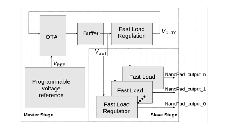
Each voltage reference circuit embedded in the NanoPads is structured as depicted in figure 12.
These regulators could have a substantial quiescent current. In this case, the total quiescent
current consumed by the large number of voltage references embedded in the WaferIC
could significantly contribute to the power consumption of the wafer-scale circuit. The use
of a master-slave architecture helps in reducing the power consumption by a factor of 16.
For example, the WaferIC contains ~1.3 million NanoPads; if each of them consumed 100
μA, this would result in a contribution to total current of 130 A, which is not acceptable. The
proposed solution is to share low-power circuitries in the master stage in a Unit-Cell. This
solution considerably reduces the power consumption of the whole wafer-scale system.
The topology of the embedded regulators in the WaferIC is such that each Unit-Cell contains
one master stage and 16 slave stages (Fig. 12). There is only one VSET reference voltage
node for the 4×4 NanoPads within the same Unit-Cell. The main function of the master stage
is to set a stable control signal VSET for all the slave stages. A programmable voltage
reference is followed by an Operational Transconductance Amplifier (OTA) in its feedback
loop, which controls the output of a buffer, followed by a fast load regulation module. The
Slave stage is controlled by VSET and provides a stable output to drive the Nanopads. The
Advanced Applications of Rapid Prototyping Technology in Modern Engineering
218
Fig. 12. Hierarchical topology of the embedded regulators in the WaferIC Unit-Cell
[Laflamme-Mayer et al., 2010].
in-situ distributed part of the regulator has a low power quiescent mode necessary due to
the fact that a full wafer device contains many copies of this circuit, most of which are
normally unused.
2.6 WaferConnect, a software tool for the WaferBoard
The rapid prototyping platform is supported by a suite of software tools called
WaferConnect. This toolbox supports a workflow defined as proposed by the Workflow
Management Coalition (WfMC, 1999). This model has been extensively used for building
general workflows (Geogakopoulos & Hornick, 1995) as well as computer-aided design
tools (Huang & Liao, 2007; Trappey et al., 2007). The proposed workflow has a total of nine
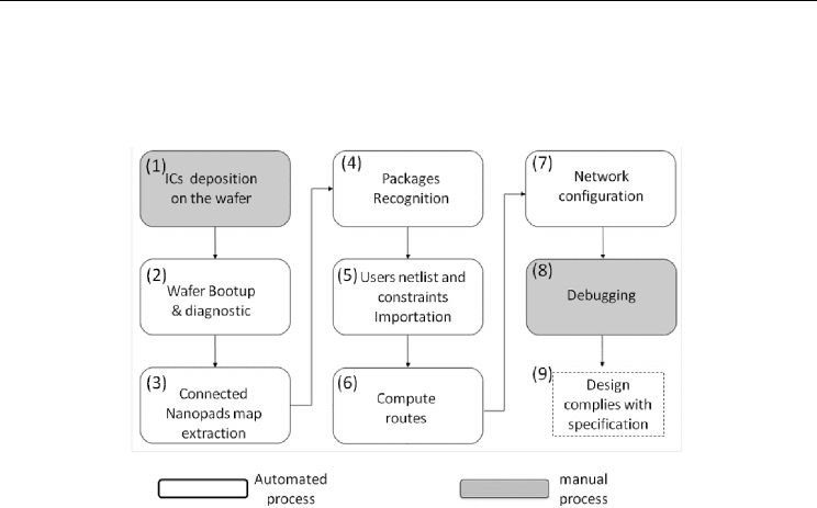
steps (see figure 13). In step 1, the user puts the required ICs on the active WaferIC surface.
Step (2) is the boot-up and diagnosis process step. At this stage the wafer is automatically
powered-up and the whole wafer is scanned to extract a defect map. That information is
forwarded to other tools designed to ensure that the system will not make use of these
defective resources. In step (3), a map of connected NanoPads (NanoPads that are in contact
with a uIC package balls) is extracted. About one million contact sensors embedded into the
WaferIC are used to extract the contact map based on shorts between adjacent NanoPads
created by a uIC solder ball.
This contact map is then used by the uIC package pin/netlist recognition process (4). The user
provides a netlist and constraints in step (5). This netlist contains information that defines
interconnections required between uICs deposited on the surface of the WaferIC. It can be
manually defined or preferably read from a standard netlist file (e.g. EDIF, GRB, Protel). The
netlist and its specified constraints are used in step (6) to compute feasible routes for each net.
The constraints supported by the proposed system are somewhat similar to those supported
by PCB routers. However, in our prototyping system, routes must be assigned to predefined
wire segments of a defect-tolerant multi-dimensional mesh interconnection network described
in (Lepercq, 2008). For instance, bus latency (timing constraints), skew, and bandwidth are
A Wafer-Scale Rapid Electronic Systems Prototyping Platform
219
other routing constraints. In step 7 the network is configured using suitable drivers. The user
then debugs his systems as part of step (8) with the support of a set of debugging tools that
will be defined as part of our future research. Finally, in step (9) of the workflow, reports are
generated to confirm compliance with the specification.
Fig. 13. The WaferBoard workflow: from WaferIC characterization up to a working
electronic system prototype.
Only two critical tools of the work flow are described here. The first is the package
recognition tool and the second is the routing tool for one type of constraints. Prior to
package recognition of the user's IC deposited on the WaferIC surface, all ball positions of
the user’s IC are estimated. The scale-space theory (Babaud, 1986) is used in the package
recognition algorithm. The position and size of each ball are estimated from the set of
NanoPads that are in contact with that ball. This problem is similar to the geometric
problem of finding the smallest bounding circle for n points in a two dimensional space
(Arvo, 1991). The package recognition is possible whenever all balls are connected to at least
two NanoPads. After estimating the balls position, a package orientation is extracted based
on two IC characteristics. Finally, the package recognition is completed by searching in a
library of known IC packages. The implemented algorithm is based on (Tuytelaars &
Mikolajezyk, 2008).
The second critical tool is the routing algorithm. In order to find the shortest path between
connected NanoPads, the interconnection network is modeled as a dense graph G(V, E) with
#E >> #V, where E is the set of WaferNet segments, V its set of cells and #S is the cardinality
of respective set S. Moreover two heuristic approaches are proposed to manage conflicts.
The first heuristic approach is called In-Order, which routes each net of the user netlist
incrementally, while the second heuristic approach computes a route independently for
each net, with the assumption of an ideal and fully functional WaferNet. A defective
interconnect resource is treated as a resource that was previously assigned to another net.
2.7 Prototypes of the WaferBoard™: three implemented test chips
A first test chip has been implemented as a proof of concept. This test chip embeds an array
of 3×3 Unit-Cells of the WaferIC (Fig. 14). It is a miniature version of the WaferIC, where
most of the functionality of the WaferIC was validated without the need to have an
Advanced Applications of Rapid Prototyping Technology in Modern Engineering
220
expensive prototype including an entire silicon wafer. Each cell contains 4×4 NanoPads,
giving a checkerboard of 12×12 NanoPads. Among the 144 NanoPads, only 22 were
accessible for testing. The others were not accessible as they were not bounded to the output
pins of the chip. Five control signals allow a JTAG scan chain to program that test chip, and
two voltage levels (3.3V and 1.8V) were needed to provide power to the user's integrated
circuit. The analog block section and programmable drivers section of each NanoPad were
validated. The digital part of the integrated circuit was implemented with standard cells.
Fig. 14. First test chip silicon die.
A test and measurement protocol has been developed: all signals transmitted to the circuit
under test were recorded by a logic analyzer that provides all the information necessary to
diagnose failures. The digital tests were performed by applying test vectors and by
measuring the output response. To validate the behavior of the WaferNet, signals were
injected into NanoPads accessible from the pins of the circuit under test. The signals injected
into NanoPads were generated by programmable waveform generators. These signals
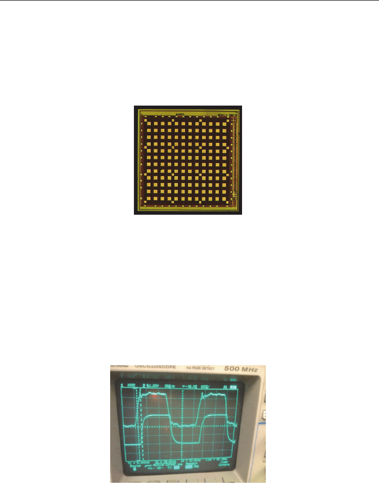
entering and leaving the WaferNet were observed using digital oscilloscopes. Figure 15
shows the results of this test on the oscilloscope. The current passing through the power
pins (VDD) and that passing through the ground (GND) were measured, as well as the
current passing through the NanoPad VDD3.3V connection.
Fig. 15. Signal propagation in the WaferNet of the first test chip.
The results obtained with the first test Chip were very significant for the WaferBoard proof
of concept. The positive results obtained demonstrated clearly that it is possible to create a
circuit embedding the WaferNet configurable network.
