Henini M. Handbook of Self Assembled Semiconductor Nanostructures for Novel devices in Photonics and Electronics
Подождите немного. Документ загружается.

Quantum Dot Superluminescent Diodes 569
ultra-narrow ( 1 Å) emission lines corresponding to the recombination of excitons, biex-
citons and other multi-excitonic states. The lines from a large ensemble of QDs (typically
10
6
–10
7
QDs are embedded in the active region of a waveguide) then merge in a broad
(30–100 nm) Gaussian-shaped emission line. At room temperature and/or high excitation
levels typical of device operation, a signifi cant homogeneous broadening (10–20 nm) of
the emission line of each QD also contributes to the total spectral width. While inhomo-
geneous broadening has always been perceived as the major obstacle to achieving high
performance in lasers, it represents a clear advantage for SLED applications. As discussed
thoroughly in section 19.2, the growth conditions can be tuned to increase the QD size
dispersion, and thus the gain spectral width. Additionally, several QD layers can be stacked
with different centre wavelengths ( “ chirped multilayers ” ), resulting in an even wider com-
bined gain spectrum.
2. Limited density of states: The number of electronic states in a QD ensemble is directly
related to their areal density (there are two spin-degenerate states on the lowest ( “ ground ” )
state for each QD). The areal density depends on the growth conditions and is typically lim-
ited to few 10
10
dots/cm
2
, particularly due to a limitation on the average strain in the sys-
tem where In-rich QDs are needed to shift the wavelength towards the 1300 nm region. By
stacking multiple layers, this can be increased to the few 10
11
dots/cm
2
range. This density
of states (DOS) is roughly a factor of 10 lower than the typical DOS in the fi rst subband
of a single QW in a comparable energy interval. This in turn results in lower maximum
modal gain corresponding to full inversion of the states (in the few 10 s cm
1
range for
QDs, as compared to 100–200 cm
1
for a single QW). This lower gain is a major limitation
for lasers, producing gain saturation and consequently poor frequency response. On the
contrary, the relatively low density of states can be an advantage for SLEDs. In fact, to
achieve population inversion over a large energy range at reasonable current levels, a
low density of states per unit energy is preferable. The ground state (GS) of a single InAs/
GaAs QD layer emitting around 1300 nm is typically fi lled with 100–200 A/cm
2
, and
a gain spectrum 100 nm wide, combining ground and excited states (ES, see right part
of Fig. 19.3 ), is obtained with less than 1 kA/cm
2
. In QWs, as mentioned above, fi lling all
states in this energy range would require 10 kA/cm
2
or more. Ultimately, the wide emis-
sion spectrum of QD SLEDs is the consequence of the relatively small density of states per
unit energy. Achieving high-output powers obviously requires a certain level of chip gain
( gL 6–10), which is nowadays achievable by stacking 10–20 layers of QDs.
19.2 QD growth for SLEDs
Large spectral width is one of the most important features of SLEDs [2, 3] , as the correspondingly
short coherence length can signifi cantly improve the spatial resolution in coherence-based sys-
tems. The large spectral width can be realized by using the techniques such as multiple-quantum
well (QW) engineering and QW intermixing [4–7]. However, increasing the SLED spectral width
over 100 nm in the 1300 nm wavelength region is still a challenge. As mentioned in section 19.1,
and originally proposed in [8] , the naturally occurring size dispersion in self-assembled growth
of quantum dots (QDs) can be benefi cial for SLEDs requiring larger spectral width. Generally,
inhomogeneous size distribution of QDs in the active region is disadvantageous for laser applica-
tions. However, for the wide spectra device applications such as SLEDs, it becomes an effective
and intrinsic merit due to the broadened gain spectrum. Size dispersion in the tens of per cent
range results in a spectral width over 100 nm from the QD active region as predicted theoretically.
Therefore, considerable efforts have been invested in developing QD SLEDs [9–22] . Initial reports
employed the uniform stacked In(Ga)As/GaAs QDs which are routinely used in laser devices,
showing a narrow spectral width and/or a short emission wavelength [10–13, 15] . To increase
the spectral width, deliberate increase of the dot size dispersion is a straightforward method
[8, 17, 21] . In addition, employing multiple QD layers with different amounts of InAs deposition
in the QDs is another option [9, 17] . Large photoluminescence (PL) spectral width over 100 nm
can be obtained by using both methods [9, 21] . However, for SLED applications, a large PL
CH019-I046325.indd 569CH019-I046325.indd 569 6/27/2008 5:21:29 PM6/27/2008 5:21:29 PM
570 Handbook of Self Assembled Semiconductor Nanostructures for Novel Devices in Photonics and Electronics
linewidth is not suffi cient, high radiative effi ciency and uniform optical gain must be obtained
across the entire spectral range. For example, varying the InAs coverage also affects the QD den-
sity, producing a non-uniform gain spectrum. As an alternative, stacking InAs-chirped multiple
QD (CMQD) structures with constant InAs coverage and varying In composition in the InGaAs
capping layer was proposed by us [4, 17] and also used by other groups [18–20] . In fact, when
the QDs are covered/surrounded by an InGaAs layer, a red shift of the emission wavelength is
observed, depending on the composition and thickness of the InGaAs layer [23, 24] . Because the
emission wavelength of each QD layer in the chirped structure can be individually controlled by a
change in the InGaAs matrix, the composite emission of the chirped structure will yield a broad
gain spectrum. In such CMQD structures, the QD areal density is not signifi cantly affected by the
InGaAs layer, so that the available gain and the wavelength are effectively decoupled and a fl at
gain spectrum can be obtained. The combined spectral broadening depends on the spectral width
of the individual QD layer, the spectral separation among each QD layer and the number of the
stacked layers. Using the CMQD structure, a composite PL spectral width of 78 nm was obtained
from the ground state (GS) of uniform QDs. Incorporating such a CMQD structure into a SLED
device structure and combining the emission from GS and excited state (ES) of QDs, SLEDs with
spectral width of 121 nm, covering from 1165 to 1286 nm, were demonstrated [14] . In such
structures a dip may appear in the spectrum between GS and ES, due to insuffi cient broadening
of the GS and ES lines. The dip can be effectively eliminated by optimizing the chirped stacking
structure and QD growth conditions. In particular, replacing uniform QDs by QDs with increased
size dispersion in the CMQD structure, smooth and broad output spectra up to 115 nm without
dip were obtained from SLEDs [17] . In the following paragraphs, the growth optimization of the
CMQD structure and single-layer InAs QDs with increased size dispersion are described.
19.2.1 Chirped multiple QD structure
High uniform InAs QDs used for laser devices have high peak gain but provide relative small gain
spectral width which limits their applicability in the SLEDs. The CMQD structure was proposed to
take advantage of the optimized gain characteristics of these QDs while increasing the total gain
linewidth in a controllable way [14] . In this part, we describe the growth of the CMQD structure.
The samples are grown on (100) GaAs substrates by using solid-source molecular beam epitaxy
(MBE). InAs QDs form by continuous deposition of InAs material (nominal thickness 3 monolay-
ers) at the growth temperature of 530°C and growth rate of 0.163 μ m/h, which are then cov-
ered by a few nm of thin InGaAs capping layer. In the CMQDs structure, the InAs/InGaAs QD
layers are separated by 40 nm GaAs barriers to avoid as much as possible strain-driven growth
coupling between different dot layers. Typical PL test structures are fi nally completed capping
the dots with a 100 nm thick GaAs barrier, and are then characterized at room temperature (RT)
exciting the dots with a 632.8 nm He–Ne laser and detecting the photoluminescence with an
uncooled InGaAs detector.
Varying indium content and thickness of the InGaAs capping allows a fi ne tuning of the PL
characteristics of each QD layer, which is very useful for the optimization of CMQDs. The depend-
ences of the RTPL peak wavelength of the samples as a function of the In composition and the
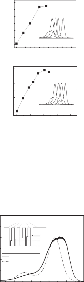
thickness of the InGaAs layer are shown in Fig. 19.4 . Insets show the normalized PL spectra
of the samples with the different In composition or the thickness of the InGaAs layer. Between
0 and 5 nm, the PL peak wavelength is proportional to the thickness of the InGaAs layer as
shown in Fig. 19.4a . The PL peak wavelength increases from 1140 to 1300 nm upon increas-
ing the InGaAs layer thickness from 0 to 6 nm. Similar behaviours are also observed when the
In composition of the InGaAs layer is changed, which is shown in Fig. 19.4b . The signifi cant PL
peak wavelength variation mainly appears in the range of In composition between 0 and 20%.
A further increase of In composition does not contribute to the further PL peak wavelength shift.
These fi ndings are in good agreement with previous reports [23, 24] . The red shift of the QD
emission with increasing In composition and thickness of the InGaAs layer can be attributed to
a reduction in the strain in the QDs [24] , to the suppressed In segregation from the QDs into the
cap layer, and to the activated spinoidal decomposition of the cap layer [25] .
CH019-I046325.indd 570CH019-I046325.indd 570 6/27/2008 5:21:29 PM6/27/2008 5:21:29 PM
Quantum Dot Superluminescent Diodes 571
By appropriately choosing In composition or thickness of the InGaAs capping layers, the emis-
sion of CMQDs should cover a wide spectral range. This idea can be easily validated by imple-
menting several QD layers with different capping properties in the same structure. Figure 19.5
(continuous line) shows the normalized RTPL spectra of a CMQD structure containing fi ve QD
layers. The In composition in the InGaAs layer is varied from 0.09 to 0.15 in steps of 0.015,
which results in a wide PL spectral width of 78 nm. The PL emission is dominated by GS transi-
tion at around 1270 nm, while the high energy tail merging with the main peak comes from ES
transition. The achieved spectral width is much larger than the typical spectral width of 44 nm
from the single-layer QD samples (dashed–dotted line), which verifi es the validity of using the
CMQD structure for spectral broadening.
PL wavelength (m)
1.26
1.20
1.32
1.14
0.1 0.2
In composition in InGaAs layer
0.30.0
0.4
900 1000 1100 1200 1300 1400
a
a: 0.00
b: 0.05
c: 0.09
d: 0.16
Wavelength (nm)
bc d
In
x
GaAs
x
(b)
1.26
PL wavelength (m)
1.20
1.32
1.14
Thickness of In
0.15
Ga
0.85
As (nm)
(a)
2
4
6
abc d
InGaAs
d(nm)
a: 0.0
b: 1.5
c: 3.0
d: 5.0
1100 1200 13001000 1400
Wavelength (nm)
810
0
12
Figure 19.4 (a) RTPL peak wavelength as a function of the thickness of the In
0.15
Ga
0.85
As layer. (b) RTPL peak
wavelength as a function of the In composition of the 5 nm thick InGaAs layer. Insets show the normalized PL spectra
of the samples with different In composition or thickness of the InGaAs layer.
1.0
0.5
GaAs barriers
1.5
0.0
1200
InGaAs
1250
1300
5 chirped layers
Single layer
QDs
1150
1350
Wavelength (nm)
Normalized intensity (a.u.)
Figure 19.5 Normalized RTPL spectra of a single layer of InAs QDs and a chirped multiple InAs QDs sample.
Inset : Schematic band diagram of the chirped QD structure.
CH019-I046325.indd 571CH019-I046325.indd 571 6/27/2008 5:21:29 PM6/27/2008 5:21:29 PM
572 Handbook of Self Assembled Semiconductor Nanostructures for Novel Devices in Photonics and Electronics
19.2.2 Increasing the inhomogeneous spectral width of a single layer of QDs
Although using the CMQD structure is effective to increase the spectral width, the number of
QD layers needed for a given total linewidth without a spectral dip, and the required accuracy
in the In content, depends on the linewidth of each layer. Increasing the inhomogeneous linew-
idth of each layer helps to obtain a broad and uniform spectrum. In this paragraph, we show the
effect of growth conditions on the linewidth, and fi nd optimized conditions for large linewidth
and high radiative effi ciency.
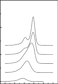
Growth temperature and amount of InAs deposited to form the dots have a strong impact
on the QD size dispersion over the ensemble and on the material quality. Figure 19.6 shows the
RTPL spectra of 2.2 ML InAs QDs deposited at various growth temperatures from 485 to 530°C
and at a growth rate of 0.1 ML/s (monolayer per second). QDs are capped with a 5 nm thick
InGaAs layer and covered by a 100 nm thick barrier. The spectral width of the QDs increases and
the PL effi ciency deteriorates when lowering the growth temperature. This can be attributed to a
reduced diffusion length of adatoms at lower growth temperatures [26] . Nucleation centres on
the epitaxial surface increase, giving rise to a high density of small dots. The size distribution of
these dots is inhomogeneous which results in the broad emission spectrum. There is an optimized
growth temperature around 510°C which gives a broad spectrum emitting near 1300 nm. Its PL
integrated intensity is comparable to that of the samples grown at higher temperature.
18
12
533°C
520°C
510°C
500°C
485°C
InAs 2.2 ML; Gr 0.1 ML/s
6
0
1.0
Intensity (a.u.)
1.1 1.2 1.3 1.4 1.5
Wavelen
g
th (m)
Figure 19.6 RTPL spectra of the 2.2 ML InAs QDs deposited at various growth temperatures for a growth rate of
0.1 ML/s.
Figure 19.7 shows the RTPL spectra of the QDs with different InAs thicknesses deposited at
growth temperatures of 485 and 510°C. With increasing InAs thickness, the PL peaks of the
samples grown at both temperatures shift systematically to the long wavelength side due to an
increased dot size. For the QDs deposited at 485°C, the spectra are broad. However, the QDs show
very low PL effi ciency and the PL emission peak is blue shifted as compared to the QDs grown
at 510°C, which prevents accessing the 1300 nm range. Although the spectral widths are large,
the QDs grown at 485°C may not be suitable for device applications. For the QDs deposited at
510°C, the spectral width of the QDs becomes small with increasing InAs thickness due to the
improved dot size uniformity [27] . A broad spectral width up to 96 nm is only obtained when
the InAs thickness is 2.2 ML due to the dot size dispersion. There might exist several groups of
QDs with different sizes, each of them emitting at different wavelengths, thereby giving rise to a
broad spectrum. The PL integrated intensities of these QDs are comparable to that of the 2.4 ML
thick InAs QD layer, which has the strongest PL intensity. In fact, 2.4 ML thick InAs QDs have
been successfully used in low threshold current density lasers, implying high radiative recombi-
nation effi ciency. It should be noticed that the PL intensity of QDs with thicknesses larger than
2.4 ML degrades, probably due to the crystal defects such as dislocations which may have been
generated in larger islands, so that they grow faster or even at the expense of the coherent ones
CH019-I046325.indd 572CH019-I046325.indd 572 6/27/2008 5:21:30 PM6/27/2008 5:21:30 PM
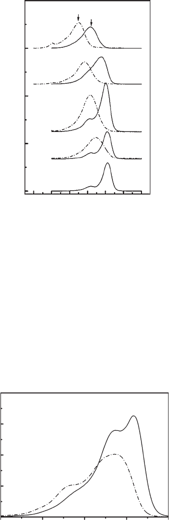
Quantum Dot Superluminescent Diodes 573
[28, 29] . In contrast, there is no dislocation in QDs with InAs thicknesses less than 2.4 ML,
implying effi cient radiative recombination.
By incorporating such dispersed InAs QDs into a CMQD structure, even larger spectral width
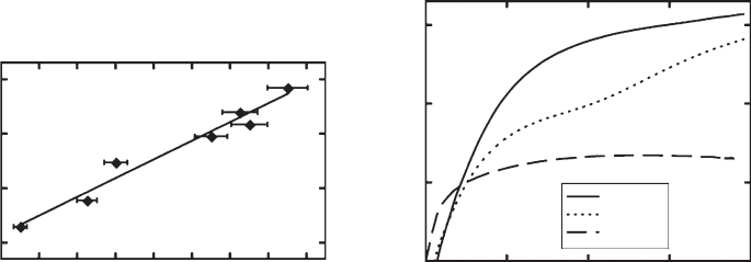
and higher gain can be expected. Two approaches were developed to stack QD layers hav-
ing chirped emission wavelength, by varying (i) the In composition in the InGaAs layer and
(ii) the InAs thickness. The RTPL spectra from the two types of structure are depicted in Fig.
19.8 . A spectral width of 91 nm (solid line) was achieved in a seven-layer stack with identical
InAs QDs (2.2 ML thick) capped by three different In compositions of an InGaAs layer (12%,
15% and 17%; structure A). The value is larger than the value of 78 nm achieved by stacking
2.4
5x
5x
10x
10x
2.8 ML
2.6 ML
2.4 ML
2.2 ML
2.0 ML
510°C
485°C
1.6
Intensity (a.u.)
0.8
3.2
0.0
1.0 1.21.1 1.3 1.40.9 1.5
Wavelength (m)
Figure 19.7 RTPL spectra of the QDs with different InAs thicknesses deposited at growth temperatures of 485°C
and 510°C.
1.5
1.0
2.0
0.5
A
B
1.04 1.12 1.20 1.28 1.36
Wavelength (m)
PL intensity (a.u.)
Figure 19.8 RTPL spectra from the two types of chirped QD structures. Structure A: seven-layer stack with
identical thick InAs QDs (2.2 ML) capped by InGaAs layers with three different In compositions (12%, 15%
and 17%); structure B: seven-layer stack with two different InAs thicknesses (2.1 and 2.2 ML) capped by InGaAs
layers with the same In compositions.
CH019-I046325.indd 573CH019-I046325.indd 573 6/27/2008 5:21:30 PM6/27/2008 5:21:30 PM

574 Handbook of Self Assembled Semiconductor Nanostructures for Novel Devices in Photonics and Electronics
chirped high uniform InAs QD layers. The largest spectral width of 124 nm was achieved in a
seven-layer stack with two different InAs thicknesses (2.1 and 2.2 ML) capped by InGaAs layers
with the same In composition (dash–dot line; structure B). These spectral widths correspond to
the combined GS ES emission. For the sample with a different InAs thickness, the deconvolved
GS spectral width is still larger than 100 nm. The optimized CMQDs with 124 nm PL linewidth
(structure B), once incorporated in an SLED device structure, result in a smooth spectral width
(GS ES) of 115 nm [17] as will be detailed in section 19.4.2.
19.2.3 Conclusions and perspectives
In this section we investigated the growth of size inhomogeneous InAs QDs and CMQD struc-
tures, in order to broaden the gain spectrum of the QD active region in the 1200–1300 nm
wavelength range. By intentionally increasing the size dispersion of InAs QDs, a broad PL spec-
tral width is achieved from a single layer of QDs. No evidence of degradation of optical proper-
ties was observed. The results confi rm that the CMQD structure is effective for devices which
need a broad-gain spectrum such as SLEDs, semiconductor optical amplifi ers and tunable lasers.
Although this discussion has been conducted on the InAs/GaAs material system for applications
in the 1300 nm region, the concepts and approaches can be easily extended to the other material
systems. In particular, it becomes possible to realize QD or quantum dash SLEDs covering various
wavelength ranges based on the material systems such as InAs QDs/quantum dashes on InP sub-
strate (1550 nm telecom wavelength) [30, 31] , InP/InGaP QDs on GaAs substrate (700–800 nm
red emission) [32, 33] , and InGaN QDs on GaN substrate (400–500 nm blue emission) [34, 35] .
19.3 Wide-spectrum InAs/GaAs QD SLEDs
19.3.1 Gain and length requirements
The typical structure of QD-SLEDs emitting in the 1.2–1.3 μ m wavelength region is made of a
certain number of QD layers separated by 35–40 nm GaAs spacers to avoid strain and coupling
effects, and embedded in the GaAs intrinsic region of a p-i-n junction. The p - and n -regions are
Al
x
Ga
1 x
As layers, which provide both optical and electrical confi nement. Starting from these
structures, devices are realized by dry-etching tilted or bent waveguides (see inset of Fig. 19.11 )
which are then passivated by BCB planarization or by steam oxidation of the exposed AlGaAs
cladding depending on the Al content in the alloy. Even though high Al content results in a high
optical confi nement, a low Al concentration can be desirable for the applications, to minimize
the reliability issues related to the aluminium oxidation and to improve the far-fi eld aspect ratio
of the emission. Ridges are a few μ m in lateral size to ensure a single lateral mode operation and
therefore an effi cient coupling into tapered single-mode fi bres (the typical coupling effi ciency
is 40–50% when the SLED operates in the amplifi cation regime), which is highly desirable for
applications. The last fabrication steps are p -contact (Ti/Pt/Au) and n -contact (Ni/Ge/Au/Ni/Au)
deposition, on top and on the substrate side, respectively, and fi nally cleaving chips of the proper
length.
The most important parameters related to the superluminescent diode output power are the
chip length L and net gain g , which relates to modal gain g
mod
and internal loss α
i
through the
relation g g
mod
α
i
. As mentioned in section 19.1.3, in a simplifi ed picture where the output
facet refl ectivities are assumed be negligible and the gain and spontaneous emission rate are
assumed to be independent from positions inside the waveguide, an exponential increase in out-
put power is expected when increasing g or L :
P
P
g
e
gL
out
sp
β
1
⎡
⎣
⎤
⎦
(19.4)
In Fig. 19.9 a the output power measured over a series of QD SLEDs with similar geometrical
characteristics (tilted waveguides with ridge widths of 3–4 μ m, 4 mm long) are reported in the
CH019-I046325.indd 574CH019-I046325.indd 574 6/27/2008 5:21:31 PM6/27/2008 5:21:31 PM
Quantum Dot Superluminescent Diodes 575
regime of emission where GS ES versus the measured maximum net gain g
max
. In spite of
the many differences between the samples (number of QD layers, cladding compositions, band-
widths, etc.) the data points show a clear exponential increase with increasing gain, in agree-
ment with Eq. 19.4, and provide a path to the achievement of high optical powers. Outputs of
10 mW or higher can be achieved only when g
max
is of the order of 18–20 cm
1
(i.e. chip gain
g
max
L 8). A fi t is reported in the plot, which was made using Eq. 19.4, where β P
sp
/g was
assumed constant and used as a fi tting parameter and L was fi xed to 4 mm. This corresponds to
a spontaneously emitted output power per unit length coupled into the guided mode at a gain of
20 cm
1
of 25 μ W mm
1
.
The effect of the device length on the L – I characteristics of tilted waveguide superlumines-
cent diodes can be observed in Fig. 19.9b . The Figure shows the L – I characteristics of three
devices fabricated from the same wafer and cleaved to 1 mm, 3 mm and 4.5 mm length. These
devices contained fi ve identical QD layers with a relatively narrow gain spectrum (20–40 nm
around 1.3 μ m, depending on the injection and amplifi cation regime) embedded into a GaAs/
Al
0.8
Ga
0.2
As waveguide. Measurements were performed in pulsed regime, at room temperature.
The output power of the 1 mm long devices saturates around 300 μ W and does not show any evi-
dent exponential characteristic in the L – I curve, which would be typical of the superluminescent
emission. The 3 mm long device in contrast reaches output powers in the mW range. For this
device two different regimes of amplifi cation can be observed, one at low and one at higher injec-
tion, which are related to recombination from different bound states in the QDs. The double expo-
nential increase is an intrinsic phenomenon in QD superluminescent diodes where the relatively
low density of states of the lower energy levels leads to state fi lling and subsequent population
of the higher energy levels. This phenomenon, which can be exploited in quantum dots for the
achievement of very large bandwidths combining the emission from different states, will be
the subject of a deeper analysis in the next paragraphs. The L – I characteristics of the 4.5 mm
long SLED reported in Fig. 19.9 b show even higher amplifi cation with output powers exceeding
10 mW mainly composed of ground state emission.
The two parameters having an important effect on the maximum modal gain
g
max
mod
are the
number of QDs contributing to the emission and the gain spectral bandwidth. The number of
dots introduced in the device active region, which are related to the DOS of the system, is directly
proportional to the modal gain. Figure 19.10 a shows
g
mod
max
measured over three samples contain-
ing fi ve, ten and 18 QD layers, at the peak wavelength, all of them having similar PL linewidths
of about 80 nm. These devices show a typical
g
mod
max
of 1–2 cm
1
per dot layer at the peak posi-
tion, which becomes slightly higher for samples with a narrower inhomogeneous broadening.
The line in the plot is a guide to the eye and has been intentionally considered sub-linear. This
is because the three waveguiding structures are not identical and the width t
opt
of the optical
1
0.1
4.5 mm
3mm
1mm
10
0.01
0.3 0.6 0.90 1.2
Current (A)
Output power (mW)
(b)
10
1
100
0.1
8
Output power (mW)
10
(a)
12 14 16 18 20622
Net gain (cm
1
)
Figure 19.9 (a) Output power measured over a series of 4 mm long, tilted QD-SLEDs in the regime of GS E S
emission, versus the corresponding maximum net gain. The data are fi tted using Eq. 19.4. (b) L – I characteristics of
tilted-waveguide SLEDs for varying device length (fabricated from the same wafer).
CH019-I046325.indd 575CH019-I046325.indd 575 6/27/2008 5:21:31 PM6/27/2008 5:21:31 PM
576 Handbook of Self Assembled Semiconductor Nanostructures for Novel Devices in Photonics and Electronics
mode in the growth direction is expected to be larger for the fi ve and ten QD layer samples, lead-
ing to a smaller confi nement factor (
g
mod
max
is inversely proportional to t
opt
). t
opt
indeed depends on
the device geometry and in particular varies proportionally to the GaAs core region thickness,
and depends on the refractive index contrast between active region and claddings (higher Al con-
tent in the claddings means higher refractive index contrast and higher confi nement and there-
fore smaller t
opt
). The fi ve QD layer sample has 80% Al concentration against 35% for the other
two samples. Also, the GaAs core region is thicker in the 18 QD layer sample than in the others.
As the spacing between different dot layers must be kept large (35–40 nm) to reduce strain and
coupling effects, the higher number of QD layers requires the growth of a thicker active region,
thus resulting in a larger t
opt
.
Once the number of QD layers is fi xed (each layer with approximately fi xed QD density of
3.10
10
cm
2
), the material gain at the peak position depends only on the shape of the broadened
density of states, whose integrated value is proportional to the total number of dots. If we con-
sider Gaussian broadenings for the GS DOS, which is usually the case for single QD layers as con-
fi rmed by the shape of the PL emission, the peak gain is reduced proportionally to the increase in
width of the broadening. The decrease in gain was observed measuring the peak gain in samples
with ten QD layers and a different PL linewidth.
g
mod
max
decreased from 20 to 15 cm
1
for a low-
excitation PL linewidth increase from 50 to 80 nm.
Number of QD layers and inhomogeneous broadening are not the only two parameters affect-
ing the gain characteristics of QD-SLEDs. The thermal redistribution of carriers over the energy
levels of a semiconductor is one of the most important parameters limiting the gain perform-
ance of devices operating at room temperature. This is true for bulk materials, where electrons
and holes occupy the continuous energy bands with quasi-Fermi distributions, but also for QDs
where the presence of close excited state energy levels may reduce the occupation and therefore
the gain of the lower energy levels. In [36] , for example, is shown how the proximity of the WL
levels (especially in the valence band) of QDs emitting around 1000 nm generates a carrier redis-
tribution reducing the maximum modal gain. Furthermore, the presence of many closely spaced
energy levels for the holes in the valence band could produce a similar effect. A few years ago the
introduction of p -doping in the QD active region was proposed as one possible solution to over-
come this problem by forcing a certain number of extra holes to be in the dots [37] . Since this
moment, many groups all over the world have been studying the effect of p-doping on the tem-
perature, gain and modulation characteristics of quantum dot lasers. Here we report the effect
of p-doping on the gain characteristics of the QD material. Later on, the effect of p-doping on
the L – I and temperature characteristics of SLEDs will be discussed. Three samples with identi-
cal epitaxial structure, grown under the same conditions, but with different doping levels in the
active region were processed into SLEDs. Each of them contains ten InAs QD layers in a GaAs
active region embedded between 1.5 μ m thick Al
0.35
Ga
0.65
As cladding layers. In sample A the dot
25
20
15
10
5
Maximum net gain (cm
1
)
30
0
(a)
Modal gain (cm
1
)
20
10
(b)
1000 2000
A
B
C
0
3000
Current density (A/cm
2
)
0
10
20
30
30
40
10 15520
QD layers
Figure 19.10 (a) Maximum modal gain versus number of QD layers for samples showing a comparable PL
linewidth. (b) Modal gain of 2 mm long and 3 μ m wide tilted ridge-waveguide devices with identical epitaxial
structure but different doping levels in the active region.
CH019-I046325.indd 576CH019-I046325.indd 576 6/27/2008 5:21:32 PM6/27/2008 5:21:32 PM
Quantum Dot Superluminescent Diodes 577
layers are separated by undoped GaAs spacers, while in samples B and C carbon doping is intro-
duced inside a thin region within each GaAs spacer (10 nm thick regions, 10 nm above each QD
layer). The doping level was estimated to correspond to the introduction of about eight and 15
extra holes per QD, for samples B and C, respectively. The spectral characteristics showed very
similar behaviour for the three samples, except for small variations in the spectral centre wave-
length (1267, 1270 and 1300 nm for samples A, B and C, respectively), demonstrating that for
the considered doping levels the dispersion of the QD density of states is not substantially modi-
fi ed. In Fig. 19.10 b the modal gain curves for TE polarization (electric fi eld perpendicular to the
growth direction) at the GS peak position versus current density are reported for the three sam-
ples. Each line interpolates a series of 80 data points obtained through the analysis of the ampli-
fi cation undertaken by a tunable laser injected in the tilted waveguides and tuned at the GS peak
wavelength. The measurements were verifi ed to be reproducible over several nominally identical
devices. The plot shows an increasing maximum modal gain with increasing doping level. The
maximum value of g
mod
for samples A, B and C is 18, 22 and 25 cm
1
, respectively. The increase
can be attributed to the modifi ed carrier distribution in the valence band due to the introduction
of several acceptors per QD, which has the effect of pushing the quasi-Fermi level deeply inside
the band, and thus increasing the hole population contributing to the gain. We note that an
increased injection current is needed in p -doped devices to achieve the same gain level. P -doping
is expected to increase monomolecular (through dopant-related defects), radiative and Auger
(through increased hole population) recombination rates. A combination of these effects is likely
to produce the shift of the gain curves towards higher current. P -doping has an impact on the
optical losses as well, through increased free carrier absorption and photon scattering due to the
introduction in the active region of doping-related crystal defects. From the measured Fabry–
Perot fringe visibility and laser thresholds in untilted devices we estimate the optical losses as
α
i
1.8 cm
1
, 3.5 and 5 cm
1
for samples A, B and C, respectively. The increase in modal gain
in p -doped structures B and C exceeds the increase in optical losses, resulting in a larger net gain
which, as we will see in the next section, results in higher output power for p -doped SLEDs.
As already discussed, the SLED output power does not depend simply on the material gain but
also on the distance travelled by photons inside the waveguide before output. In tilted devices this
can be assumed to be equal to the device length (single-pass amplifi cation). In contrast, combin-
ing the low refl ectivity of one facet with the high refl ectivity of the opposite, in bent devices the
photon may cover a larger length than the cavity length before output. This leads to higher light
amplifi cation and therefore higher output power, provided that the waveguide curvature does
not introduce signifi cantly higher internal loss. With this purpose bent stripes were realized by
using an arc of circumference whose tangents at the two end points are 7 ° tilted and perpendicu-
lar to the opposite facets of a 2 mm long cavity, respectively. Longer cavities were also realized
by adding a straight piece of waveguide to the perpendicular facet side. This combines the low
refl ectivity of the tilted facet with the high refl ectivity of the perpendicular facet so that the light
travelling inside the waveguide may experience double-pass amplifi cation. A comparison between
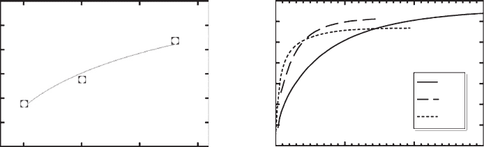
the L – I characteristics of a 2 mm long bent and 2 mm long tilted waveguide are reported in Fig.
19.11 . Both devices were fabricated with the same process and from the same wafer, thus dem-
onstrating that the bent structure is effective in increasing the light amplifi cation if compared to
a single-pass guide. While the output power of the tilted waveguide is limited to few mW at high
injection, bent waveguides achieve 30 mW at the same injection.
In the following paragraphs, we will fi rst describe the characteristics of SLEDs fabricated from
samples with a narrow gain, optimized for emission at 1.3 μ m, as they are the standard gain
material for high-performance QD lasers. This results in devices with narrow optical bandwidths
but at the same time provides useful information for the understanding of the device character-
istics. Then, in section 19.3.3 we will discuss the properties of SLEDs with chirped active regions
showing that through the optimization of growth conditions – as discussed in section 19.2 – the
device output may exhibit bandwidths larger than 100 nm. The large bandwidth is obtained in a
regime of two-state emission (GS ES) that, for optimized chirping, results in a smooth spectral
superposition (fl at top). The coherence properties and temperature characteristics of both types
of devices are addressed in sections 19.3.4 and 19.3.5.
CH019-I046325.indd 577CH019-I046325.indd 577 6/27/2008 5:21:32 PM6/27/2008 5:21:32 PM
578 Handbook of Self Assembled Semiconductor Nanostructures for Novel Devices in Photonics and Electronics
19.3.2 Narrow-gain devices
In this paragraph we report the spectral and L – I characteristics of SLEDs realized from samples
containing fi ve and ten identical QD layers. More details about these devices can be found in [13,
15] . Tilted-ridge SLEDs fabricated from these samples were mounted p-side up on a temperature
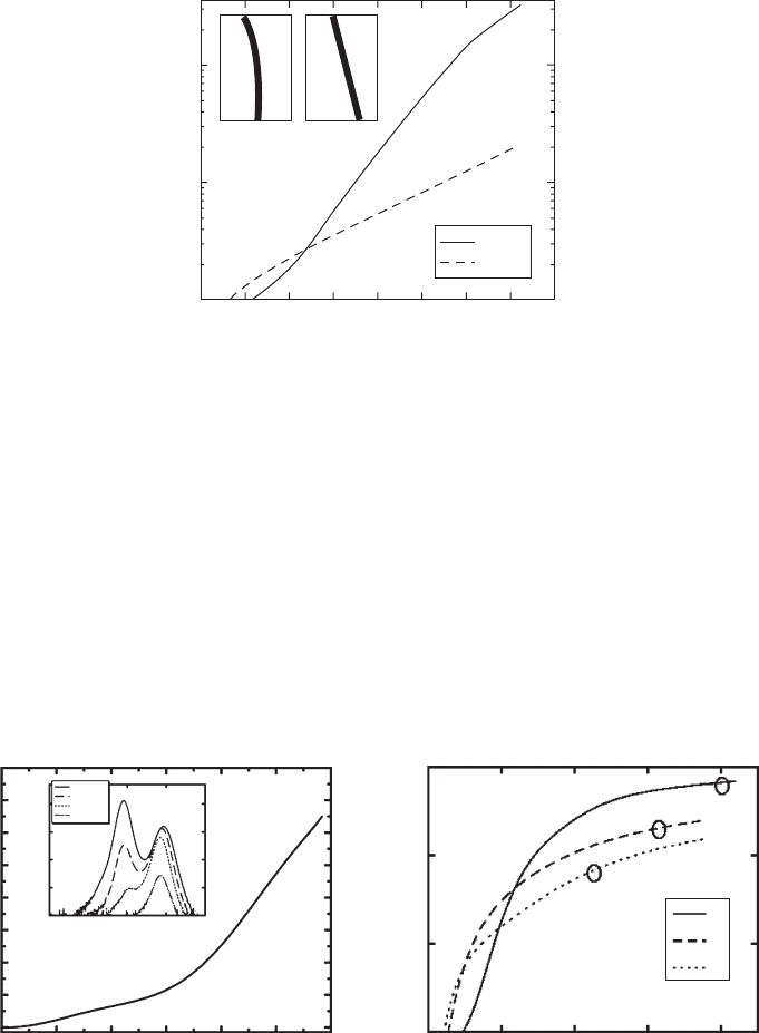
controlled heat-sink, and tested under pulsed operation. In Fig. 19.12a the L – I characteristics of
a 3 mm long SLED are reported for the heat-sink temperature of 10°C. Two separated superlinear
behaviours can be identifi ed in the curve: one at low injection (0–200 mA) and one at higher
injection (600–800 mA) which are related to the recombination from GS and ES energy levels of
the dot. The superlinear increase in output power together with the high power (of the order of
10 mW at high injection) are the signature of operation in the gain regime.
16
14
12
10
8
6
4
2
0
0 0.2 0.4 0.6 0.8 1 1.2
Current (A)
1200 mA
600 mA
300 mA
100 mA
10
1
10
2
10
3
10
4
10
5
1000 1100 1200 1300 1400
26 nm FWHM
22 nm FWHM
Output power (mW)
Wavelength (nm)
Intensity (a.u.)
(a)
0 200 400 600 800
0.1
1
10
100
Power (mW)
Current (mA)
C
B
A
(b)
Figure 19.12 (a) L – I characteristics of a 3 mm long tilted ridge-waveguide SLED containing fi ve QD layers,
measured at 10°C in pulsed regime. The corresponding spectra are reported in the inset. (b) L – I characteristics of
4 mm long tilted ridge-waveguide SLEDs containing ten QD layers and different p -doping levels in the active region.
The circles identify the regime of emission where GS and ES contributions to the spectra are comparable.
10
1
0.1
0
100
200 300 400
500
600 700 800
Current (mA)
Output power (mW)
Bent
Tilted
Bent
Tilted
Figure 19.11 Bent versus tilted SLED structures (2 mm long chips): bent waveguides allow the achievement of
higher output powers at the same injection levels. A schematic drawing of the two structures is reported in the inset.
A better understanding of the L – I characteristics can be achieved observing the corresponding
spectra reported in the inset of Fig. 19.12a . At low injection the GS provides the main contribu-
tion to the emission with 26 nm full width at half maximum (FWHM) and up to 2 mW output
power. At higher currents this emission saturates because of the GS fi lling and a second line due
to recombination from the fi rst ES appears. This line is eventually dominant (exceeding 10 mW)
CH019-I046325.indd 578CH019-I046325.indd 578 6/27/2008 5:21:32 PM6/27/2008 5:21:32 PM