Gibilisco S. Teach Yourself Electricity and Electronics
Подождите немного. Документ загружается.

Test: Part 2 311
(d) C = 60 µF and R = 25 Ω.
(e) L = 60 µH and R = 25 Ω.
42. Suppose two pure sine waves have no dc components, have the same frequency, and have the
same peak-to-peak voltages, but they cancel each other out when combined. What is the phase
difference between the waves?
(a) 45°
(b) 90°
(c) 180°
(d) 270°
(e) 360°
43. Suppose a series RC circuit has a resistance of 50 Ω and a capacitive reactance of −37 Ω.
What is the phase angle?
(a) 37°
(b) 53°
(c) −37°
(d) −53°
(e) It cannot be calculated from the data given.
44. Suppose a 200-Ω resistor is in series with a coil and capacitor, such that X
L
= 200 Ω and X
C
=
−100 Ω. What is the complex impedance?
(a) 200 − j100
(b) 200 − j200
(c) 200 + j100
(d) 200 + j200
(e) Impossible to determine from the data given
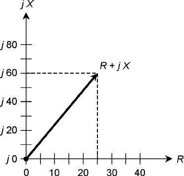
Test 2-2 Illustration for
Part 2 Test
Question 41.
45. The characteristic impedance of a transmission line
(a) is negative imaginary.
(b) is positive imaginary.
(c) depends on the frequency.
(d) depends on the construction of the line.
(e) depends on the length of the line.
46. Suppose the period of a pure sine wave is 2 × 10
−8
s. What is the frequency?
(a) 2 × 10
8
Hz
(b) 20 MHz
(c) 50 kHz
(d) 50 MHz
(e) 500 MHz
47. Suppose a series RC circuit has a resistance of 600 Ω and a capacitance of 220 pF. What is the
phase angle?
(a) −20°
(b) 20°
(c) −70°
(d) 70°
(e) Not determinable from the data given
48. A capacitor with a negative temperature coefficient
(a) works less well as the temperature increases.
(b) works better as the temperature increases.
(c) heats up as its value is made larger.
(d) cools down as its value is made larger.
(e) exhibits increasing capacitance as the temperature drops.
49. Suppose three coils are connected in parallel. Each has an inductance of 300 µH. There is no
mutual inductance. What is the net inductance?
(a) 100 µH
(b) 300 µH
(c) 900 µH
(d) 17.3 µH
(e) 173 µH
50. Suppose a coil has 100 Ω of inductive reactance at 30.0 MHz. What is its inductance?
(a) 0.531 µH
(b) 18.8 mH
(c) 531 µH
(d) 18.8 µH
(e) It can’t be found from the data given.
312 Test: Part 2
3
PART
Basic Electronics
Copyright © 2006, 2002, 1997, 1993 by The McGraw-Hill Companies, Inc. Click here for terms of use.
This page intentionally left blank
SINCE THE 1960S, WHEN THE TRANSISTOR BECAME COMMON IN CONSUMER DEVICES, SEMICONDUCTORS
have acquired a dominating role in electronics. The term semiconductor arises from the ability of these
materials to conduct some of the time, but not all the time. The conductivity can be controlled to
produce effects such as amplification, rectification, oscillation, signal mixing, and switching.
The Semiconductor Revolution
Decades ago, vacuum tubes, also known as electron tubes, were the only devices available for use as
amplifiers, oscillators, detectors, and other electronic circuits and systems. A typical tube (called a
valve in England) ranged from the size of your thumb to the size of your fist. They are still used in
some power amplifiers, microwave oscillators, and video display units.
Tubes generally require high voltage. Even in modest radio receivers, 100 V to 200 V dc was re-
quired when tubes were employed. This mandated bulky power supplies, and created an electrical
shock hazard. Nowadays, a transistor of microscopic dimensions can perform the functions of a
tube in most situations. The power supply can be a couple of AA cells or a 9-V transistor battery.
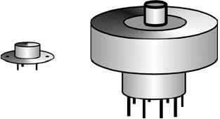
Even in high-power applications, transistors are smaller and lighter than tubes. Figure 19-1 is a
size comparison drawing between a transistor and a vacuum tube for use in an AF or RF power am-
plifier.
Integrated circuits (ICs), hardly larger than individual transistors, can do the work of hundreds
or even thousands of vacuum tubes. An excellent example of this technology is found in personal
computers and the peripheral devices used with them.
315
19
CHAPTER
Introduction to
Semiconductors
19-1 A power-amplifier
transistor (at left) is
much smaller than a
vacuum tube of
comparable power-
handling capacity
(right).
Copyright © 2006, 2002, 1997, 1993 by The McGraw-Hill Companies, Inc. Click here for terms of use.
Semiconductor Materials
Various elements, compounds, and mixtures can function as semiconductors. The two most com-
mon materials are silicon and a compound of gallium and arsenic known as gallium arsenide (often
abbreviated GaAs). In the early years of semiconductor technology, germanium formed the basis for
many semiconductors; today it is seen occasionally, but not often. Other substances that work as
semiconductors are selenium, cadmium compounds, indium compounds, and the oxides of certain
metals.
Silicon
Silicon (chemical symbol Si) is widely used in diodes, transistors, and integrated circuits. Generally,
other substances, or impurities, must be added to silicon to give it the desired properties. The best
quality silicon is obtained by growing crystals in a laboratory. The silicon is then fabricated into
wafers or chips.
Gallium Arsenide
Another common semiconductor is the compound gallium arsenide. Engineers and technicians call
this material by its acronym-like chemical symbol, GaAs, pronounced “gas.” If you hear about “gas-
fets” and “gas ICs,” you’re hearing about gallium-arsenide technology.
GaAs devices require little voltage, and will function at higher frequencies than silicon devices
because the charge carriers move faster through the semiconductor material. GaAs devices are rela-
tively immune to the effects of ionizing radiation such as X rays and gamma rays. GaAs is used in
light-emitting diodes (LEDs), infrared-emitting diodes (IREDs), laser diodes, visible-light and
infrared (IR) detectors, ultra-high-frequency (UHF) amplifying devices, and a variety of integrated
circuits.
Selenium
Selenium exhibits conductivity that varies depending on the intensity of visible light or IR radiation
that strikes it. All semiconductor materials exhibit this property, known as photoconductivity, to
some degree; but in selenium the effect is especially pronounced. For this reason, selenium is useful
for making photocells. Selenium is also used in certain types of rectifiers. A rectifier is a component
or circuit that converts ac to pulsating dc.
A significant advantage of selenium is the fact that it is electrically rugged. Selenium-based
components can withstand brief transients, or spikes, of abnormally high voltage, better than com-
ponents made with most other semiconductor materials.
Germanium
Pure elemental germanium is a poor electrical conductor. It becomes a semiconductor only when
impurities are added. Germanium was used extensively in the early years of semiconductor technol-
ogy. Some diodes and transistors still use it.
A germanium diode has a low voltage drop (0.3 V, compared with 0.6 V for silicon and 1 V
for selenium) when it conducts, and this makes it useful in some situations. But germanium is
easily destroyed by heat. Extreme care must be used when soldering the leads of a germanium
component.
316 Introduction to Semiconductors
Metal Oxides
Certain metal oxides have properties that make them useful in the manufacture of semiconductor
devices. When you hear about MOS (pronounced “moss”) or CMOS (pronounced “sea moss”)
technology, you are hearing about metal-oxide semiconductor and complementary metal-oxide semi-
conductor devices, respectively.
An advantage of MOS and CMOS devices is the fact that they need almost no power to function.
They draw so little current that a battery in a MOS or CMOS device lasts just about as long as it would
on the shelf. Another advantage is high speed. This allows operation at high frequencies in RF equip-
ment, and makes it possible to perform many switching operations per second for use in computers.
Certain types of transistors, and many kinds of ICs, make use of this technology. In integrated
circuits, MOS and CMOS allow for a large number of discrete diodes and transistors on a single
chip. Engineers would say that MOS/CMOS has high component density.
The biggest problem with MOS and CMOS technology is the fact that the devices are easily
damaged by static electricity. Care must be used when handling components of this type. Techni-
cians working with MOS and CMOS components must literally ground themselves by wearing a
metal wrist strap connected to a good earth ground. Otherwise, the electrostatic charges that nor-
mally build up on their bodies can destroy MOS and CMOS components when equipment is con-
structed or serviced.
Doping and Charge Carriers
For a semiconductor material to have the properties necessary in order to function as electronic
components, impurities are usually added. The impurities cause the material to conduct currents in
certain ways. The addition of an impurity to a semiconductor is called doping. Sometimes the im-
purity is called a dopant.
Donor Impurities
When an impurity contains an excess of electrons, the dopant is called a donor impurity. Adding
such a substance causes conduction mainly by means of electron flow, as in an ordinary metal such
as copper or aluminum. The excess electrons are passed from atom to atom when a voltage exists
across the material. Elements that serve as donor impurities include antimony, arsenic, bismuth, and
phosphorus. A material with a donor impurity is called an N-type semiconductor, because electrons
have negative (N) charge.
Acceptor Impurities
If an impurity has a deficiency of electrons, the dopant is called an acceptor impurity. When a sub-
stance such as aluminum, boron, gallium, or indium is added to a semiconductor, the material con-
ducts by means of hole flow. A hole is a missing electron—or more precisely, a place in an atom where
an electron should be, but isn’t. A semiconductor with an acceptor impurity is called a P-type semi-
conductor, because holes have, in effect, a positive (P) charge.
Majority and Minority Carriers
Charge carriers in semiconductor materials are either electrons, each of which has a unit negative
charge, or holes, each of which has a unit positive charge. In any semiconductor substance, some
Doping and Charge Carriers 317
of the current takes the form of electrons passed from atom to atom in a negative-to-positive direc-
tion, and some of the current occurs as holes that move from atom to atom in a positive-to-negative
direction.
Sometimes electrons account for most of the current in a semiconductor. This is the case if the
material has donor impurities, that is, if it is of the N type. In other cases, holes account for most of
the current. This happens when the material has acceptor impurities, and is thus of the P type. The
dominating charge carriers (either electrons or holes) are called the majority carriers. The less abun-
dant ones are called the minority carriers. The ratio of majority to minority carriers can vary, depend-
ing on the way in which the semiconductor material has been manufactured.
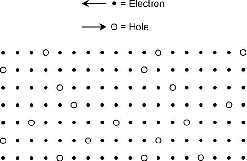
Figure 19-2 is a simplified illustration of electron flow versus hole flow in a sample of N-type
semiconductor material, where the majority carriers are electrons and the minority carriers are
holes. The solid black dots represent electrons. Imagine them moving from right to left in this
illustration as they are passed from atom to atom. Small open circles represent holes. Imagine them
moving from left to right in the illustration. In this particular example, the positive battery or
power-supply terminal (or “source of holes”) would be out of the picture toward the left, and the
negative battery or power-supply terminal (or “source of electrons”) would be out of the picture to-
ward the right.
The P-N Junction
Merely connecting up a piece of semiconducting material, either P or N type, to a source of current
can be interesting, and a good subject for science experiments. But when the two types of material
are brought together, the boundary between them, called the P-N junction, behaves in ways that
make semiconductor materials truly useful in electronic components.
The Semiconductor Diode
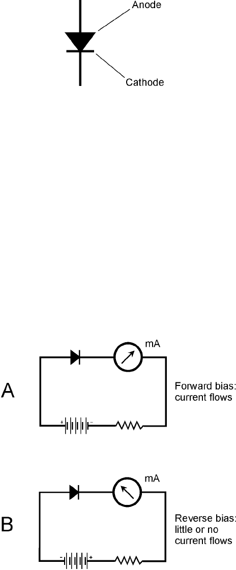
Figure 19-3 shows the schematic symbol for a semiconductor diode, formed by joining a piece of
P-type material to a piece of N-type material. The N-type semiconductor is represented by the short,
straight line in the symbol, and is called the cathode. The P-type semiconductor is represented by the
arrow, and is called the anode.
318 Introduction to Semiconductors
19-2 Pictorial representation
of hole flow. Solid
black dots represent
electrons, moving in
one direction. Open
circles represent holes,
moving in the opposite
direction.
In the diode as shown in Figure 19-3, electrons can move easily in the direction opposite the
arrow, and holes can move easily in the direction in which the arrow points. But current cannot,
under most conditions, flow the other way. Electrons normally do not move with the arrow, and
holes normally do not move against the arrow.
If you connect a battery and a resistor in series with the diode, you’ll get a current to flow if the
negative terminal of the battery is connected to the cathode and the positive terminal is connected
to the anode, as shown in Fig. 19-4A. No current will flow if the battery is reversed, as shown in
Fig. 19-4B. (The resistor is included in the circuit to prevent destruction of the diode by excessive
current.)
It takes a specific, well-defined minimum applied voltage for conduction to occur through a
semiconductor diode. This is called the forward breakover voltage. Depending on the type of mate-
rial, the forward breakover voltage varies from about 0.3 V to 1 V. If the voltage across the junction
is not at least as great as the forward breakover voltage, the diode will not conduct, even when it is
connected as shown in Fig. 19-4A. This effect, known as the forward breakover effect or the P-N
junction threshold effect, can be of use in circuits designed to limit the positive and/or negative peak
voltages that signals can attain. The effect can also be used in a device called a threshold detector, in
which a signal must be stronger than a certain amplitude in order to pass through.
The P-N Junction 319
19-3 Schematic symbol for
a semiconductor
diode.
19-4 Series connection of a
battery, a resistor, a
current meter, and a
diode. At A, forward
bias results in a flow of
current. At B, reverse
bias results in no
current.
How the Junction Works
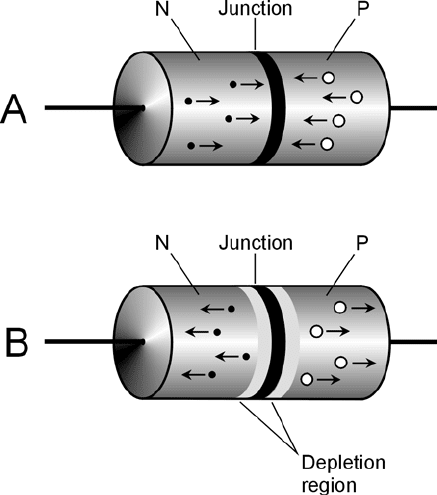
When the N-type material is negative with respect to the P type, as in Fig. 19-4A, electrons flow eas-
ily from N to P. The N-type semiconductor, which already has an excess of electrons, receives more;
the P-type semiconductor, with a shortage of electrons, has some more taken away. The N-type ma-
terial constantly feeds electrons to the P type in an attempt to create an electron balance, and the
battery or power supply keeps robbing electrons from the P-type material. This condition is illus-
trated in Fig. 19-5A, and is known as forward bias. Current can flow through the diode easily under
these circumstances.
When the battery or dc power-supply polarity is switched so the N-type material is positive
with respect to the P type, the situation is called reverse bias. Electrons in the N-type material are
pulled toward the positive charge pole, away from the P-N junction. In the P-type material, holes
are pulled toward the negative charge pole, also away from the P-N junction. The electrons are the
majority carriers in the N-type material, and the holes are the majority carriers in the P-type mate-
rial. The charge therefore becomes depleted in the vicinity of the P-N junction, and on both sides
of it, as shown in Fig. 19-5B. This zone, where majority carriers are deficient, is called the depletion
region. A shortage of majority carriers in any semiconductor substance means that the substance
cannot conduct well. Thus, the depletion region acts like an electrical insulator. This is why a semi-
conductor diode will not normally conduct when it is reverse-biased. A diode is, in effect, a one-way
current gate—usually!
Junction Capacitance
Some P-N junctions can alternate between conduction (in forward bias) and nonconduction (in re-
verse bias) millions or billions of times per second. Other junctions are slower. The main limiting
320 Introduction to Semiconductors
19-5 At A, forward bias of a
P-N junction. At B,
reverse bias of the
same junction. Solid
black dots represent
electrons. White dots
represent holes. Arrows
indicate direction of
charge-carrier
movement.
