Gersten J.I., Smith F.W. The Physics and Chemistry of Materials
Подождите немного. Документ загружается.

SEMICONDUCTORS 119
surfaces, to be discussed later. Typical measured minority-carrier lifetimes in extrinsic
Si are 1 to 100
µs, whereas in extrinsic GaAs they are 1 to 50 ns.
Minority-carrier recombination times can be on the order of picoseconds in amor-
phous semiconductors, due to the strong disorder and very high concentrations of
defects. Amorphous semiconductors can therefore be very “fast” materials with regard
to the speed of their response to external carrier excitation. The recombination times
(
p
and (
n
in crystalline semiconductors are typically much longer than the average
collision times h(i³10
13
to 10
12
s.
Electron–hole recombination in the indirect-bandgap semiconductors Si, Ge, and
GaP is much more likely to occur via the participation of defects and surfaces. These
two extrinsic recombination mechanisms are discussed next.
Defect-Mediated Recombination. Defects such as metallic impurities and dislo-
cations disturb the periodic potential of the lattice and as a result introduce energy
levels deep within the energy gap of the semiconductor, often near midgap, as shown
in Fig. 11.22 for Si. The recombination rate will then be enhanced when electrons in
the conduction band fall first into the empty defect levels and then fall further into
empty levels in the valence band. The defect-mediated recombination rate is propor-
tional to the concentration of defects that have empty energy levels in the energy gap.
These defects with deep levels in the gap are often referred to as recombination centers
or traps. The carrier wavefunctions associated with traps are highly localized. While
band-to-band recombination can be expected to be the dominant recombination process
at high temperatures when n, p, and their product np are all large due to thermal
generation, defect-mediated recombination will often be the dominant recombination
mechanism at lower temperatures.
The case of defect levels with two charge states, neutral (unoccupied) and negative
(occupied by a single electron), has been treated in detail by Hall and by Shockley and
Read.
†
Only a brief outline is presented here. The key idea is that empty defect levels
near midgap will greatly increase the rate of recombination of electrons and holes due
to the fact that such transitions are enhanced when the energy involved is smaller (e.g.,
³ E
g
/2) than the energy E
g
for band-to-band recombination.
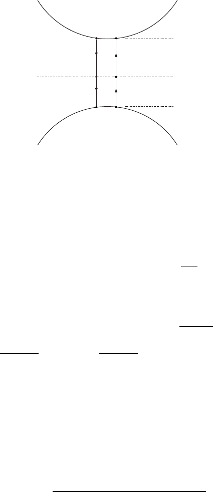
The possible transitions involving electrons and holes resulting from a defect level
at the energy E
t
in the gap are presented in Fig. W11.11. Transitions 1 and 2 corre-
spond to the capture by the defect of an electron from the conduction band and of a
hole from the valence band, respectively, with transitions 1 C2 together resulting
in the recombination of an electron with a hole. Transitions 3 and 4 correspond
to the emission by the defect of a hole into the valence band and of an electron
into the conduction band, respectively, with transitions 3 C 4 together resulting in the
creation of an electron–hole pair. These defect levels are also effective in deactivating
donors and acceptors in semiconductors through the capture of the donor electrons and
acceptor holes.
When the rates of the individual transitions 1 to 4 are considered along with the
probabilities of occupation of the levels, the following results are obtained for the
steady-state emission probabilities of electrons and holes from the levels [for details,
see Grove (1967)].
†
R. N. Hall, Phys. Rev., 87, 387 (1952); W. Shockley and W. T. Read, Phys. Rev., 87, 835 (1952).
120 SEMICONDUCTORS
E
g
E
t
1
Electron
capture
Electron
emission
Hole
capture
Hole
emission
4
23
E = 0
Figure W11.11. Possible transitions involving electrons and holes and resulting from a defect
level at the energy E
t
in the gap. 1, Capture of an electron; 2, capture of a hole; 3, emission of
a hole; 4, emission of an electron.
Absence of Carrier Injection (G
I
D 0). The total emission rates for holes and electrons,
transitions 3 and 4, respectively, will be proportional to the following rates:
Transition 3:
hole emission rate e
p
D v
pth
p
N
v
exp
E
t
k
B
T
W11.26
Transition 4:
electron emission rate e
n
D v
nth
n
N
c
exp
E
g
E
t
k
B
T
W11.27
Here
v
pth
D
3k
B
T/m
Ł
h
and v
nth
D
3k
B
T/m
Ł
e
are the thermal velocities,
p
and
n
are the capture cross sections (³ 10
19
m
2
), and N
v
and N
c
are the effective densities
of states defined in Eq. (11.27), all for holes and electrons, respectively. The rates
of transitions 1 to 4 will also be proportional to the concentration of recombination
centers N
t
and to the probabilities expressed in terms of the Fermi–Dirac distribution
function that the final state is empty.
Low-Level Carrier Injection (G
I
> 0). Net recombination rate due to defects (assuming
that
n
D
p
D ):
U D R G
T
D
v
nth
v
pth
1/2
N
t
pn n
2
i
n C p C 2n
i
cosh[2E
t
E
g
/2k
B
T]
.W11.28
Here the carrier concentrations n and p depend on the injection rate G
I
,andN
t
is the
density of defects whose energy levels lie in the gap at an energy E
t
. The recombination
rate U has its maximum value for a given G
I
when E
t
D E
g
/2 (i.e., when the hyperbolic
cosine term in the denominator has its minimum value of unity). Thus recombination
centers or traps are most effective when their energy levels are located at midgap.

SEMICONDUCTORS 121
In an n-type semiconductor the defect energy levels at E
t
will ordinarily be occupied
by electrons since n × p. These electrons can be thought of as originating directly
from the donor levels. As a result, the effective donor concentration will be reduced
to N
d
N
t
in an n-type semiconductor containing a concentration N
t
of recombina-
tion centers. This phenomenon, which can also occur in p-type semiconductors, is
known as majority-carrier removal and leads to an increase of the resistivity of the
semiconductor.
The lifetime for the minority-carrier holes in an n-type semiconductor containing
recombination centers and under low-level injection is determined by their rate of
capture by these centers. The capture lifetime can be shown to be given by
(
p
D
1
p
v
pth
N
t
.W11.29
A similar equation for (
n
is valid for electrons in a p-type semiconductor but with
p
and v
pth
replaced by
n
and v
nth
. As soon as a hole is captured by a recombi-
nation center in an n-type semiconductor (transition 2 in Fig. W11.11), an electron
will be captured essentially immediately by the center (transition 1) due to the high
concentration of electrons in the conduction band. Thus the rate-limiting step for elec-
tron–hole recombination in a semiconductor containing recombination centers will be
the capture by the center of minority carriers. As a result, the minority-carrier lifetime
is an important parameter in semiconductor devices.
The minority-carrier lifetimes (
p
or (
n
can be determined experimentally from the
decay of the photoconductivity associated with photogenerated carriers. This lifetime
is typically much longer than h(i, the average elastic scattering time, which determines
the mobility of the charge carriers. The minority-carrier lifetimes (
p
or (
n
can be
determined reliably only for low levels of illumination or injection.
Surface Recombination. The recombination rates of electrons and holes can be
enhanced at the surface of a semiconductor due to the presence of surface states (i.e.,
electron energy levels lying deep within the energy gap which result from distortions
near the surface of the bulk periodic lattice potential). These levels in the energy gap can
arise from broken or reconstructed chemical bonds at the surface of the semiconductor,
as described in Chapter 19. When surface recombination is important, the electron and
hole concentrations will vary spatially and both will be depressed near the surface of
the semiconductor due to the enhanced recombination occurring there.
The recombination rate per unit area of surface for holes in an n-type semicon-
ductor under low-level injection is usually taken to be proportional to (p
n
p
0
)and
of the form
R
surface
D s
p
p
n
p
0
, W11.30
where s
p
is the surface recombination velocity and has units of m/s. This velocity can
be shown to be given by
s
p
D
p
v
pth
N
ts
,W11.31
where N
ts
is the concentration of recombination centers per unit area at the surface.
Typical values of s
p
for Si surfaces are ³ 1 m/s but can be as high as 10
3
m/s. The value
of s
p
for Si can be reduced to 10
2
to 10
1
m/s when the Si surface is oxidized. The
122 SEMICONDUCTORS
removal of these centers by passivation of the surface (e.g., by growing or depositing a
surface film of a-SiO
2
) is an important step in the fabrication of semiconductor devices
(see Chapter W21). The spatial dependence p(x) of the hole concentration near the
surface due to recombination can be obtained by solving the continuity equation (11.65)
with the incorporation of an appropriate hole diffusion term. In addition, the effect of
a space-charge region near the surface on the recombination rate can be determined.
For details of these calculations, see Grove (1967).
The total minority-carrier recombination rate in a semiconductor is given by
1
(
D
1
(
r
C
1
(
nr
,W11.32
where (
r
and (
nr
are the radiative and nonradiative lifetimes, respectively. Another
useful expression for 1/(
p
in an n-type semiconductor when all three types of recom-
bination are important is
1
(
p
D k
1
n
0
C
p
v
pth
N
t
C
p
v
pth
N
ts
d
s
,W11.33
where Eqs. (11.72), (W11.29), and (W11.31) have been used. Here d
s
is the width of
the region near the surface where surface recombination is effective.
W11.8 Transistors
The relative suitability of semiconductors for given types of applications is often eval-
uated on the basis of relevant figures of merit (FOMs) which are specific functions
of the properties of the semiconductors. For example, the Johnson FOM for the
power capacity of high-frequency devices is JM D E
c
v
sat
/,
2
,theKeyes FOM for
the thermal dissipation capacity of high-frequency devices is KM D !
p
v
sat
//,and
the Baliga FOM for power-loss minimization at high frequencies is BHFM D E
2
c
.In
these expressions E
c
is the critical electric field for breakdown, v
sat
the saturated carrier
drift velocity, ! the thermal conductivity, / the permittivity, and the carrier mobility.
Figures of merit for various semiconductors, normalized to 1 for Si, are presented in
Table W11.3.
TABLE W11.3 Figures of Merit for Various Semiconductors
E
g
JM KM BHFM
Semiconductor (eV) E
c
v
sat
/,
2
!
p
v
sat
// E
2
c
Si 1.11 1.0 1.0 1.0
InP 1.27 13 0.72 6.6
GaAs 1.42 11 0.45 16
GaP 2.24 37 0.73 38
3C-SiC (ˇ-SiC) 2.3 110 5.8 12
4H-SiC 3.27 410 5.1 34
C (diamond) 5.4 6220 32 850
Source: Data from T. P. Chow and R. Tyagi, IEEE Trans. Electron Devices, 41, 1481 (1994).

SEMICONDUCTORS 123
The entries in Table W11.3 indicate that the semiconductors listed with wider
bandgaps than Si offer in many cases potential order-of-magnitude improvements
in performance in high-power, high-frequency electronic applications. This is to be
expected since E
c
is observed to increase with increasing E
g
.
Transistors are semiconductor electronic devices with at least three electrodes, as
shown in Fig. W11.12 for the case of an npn bipolar junction transistor. The term
bipolar refers to the fact that both electrons and holes flow within the device in
response to applied voltages. Other transistor structures in which only electrons or
holes respond to applied voltages include field-effect transistors (FETs) such as the
junction FET and the metal–oxide–semiconductor FET (MOSFET). A wide variety
of structures are employed for transistors, depending on the application (e.g., ampli-
fication or switching involving high frequency, high power, high speed, etc.). Only a
brief outline of transistor action and the most important transistor structures will be
presented here.
Bipolar Junction Transistor. A Si bipolar junction transistor consists physically of
three distinct regions of Si with different types and levels of doping and separated by
p-n junctions of opposite polarity in series with each other. These three regions can
either be embedded in a single piece of Si or can consist of layers of Si grown epitax-
ially on a Si substrate. The latter configuration is found in planar device technology,
as described in Chapter W21. The two possible types of bipolar junction transistors
are npn and pnp. The physical principles of operation are the same in each type, but
with electrons and holes switching roles, and so on. When the npn junction transistor
is connected to an external circuit as shown in Fig. W11.13, the left-hand side is the
n-type emitter, the central region is the p-type base, and the right-hand side is the
n-type collector. The built-in electric fields in the n-p and p-n junctions are in oppo-
site directions, as shown in Fig. W11.12. The electron energy bands at zero bias are
shown for the case when all three regions are nondegenerate, but with the emitter more
heavily doped (i.e., n
C
) than the base or the collector.
The operation of the npn transistor consists of forward biasing of the emitter –base
n-p junction and a stronger reverse biasing of the base–collector p-n junction, as shown
in Fig. W11.13. The electron energy bands are also shown for the npn transistor when
biased as described above. Electrons are injected from the emitter into the base where
E
np
E
c
E
F
E
v
E
pn
E
np
E
pn
np
p
(a)
(b)
n
n
+
n
Figure W11.12. An npn bipolar junction transistor: (a) directions of the built-in electric fields
at the two junctions; (b) electron energy bands across the transistor at zero bias.
124 SEMICONDUCTORS
− −
− − − −
+
− −
Emitter Base Collector
n
+
n
+
n
I
c
I
e
V
bc
V
eb
V= 0
I
b
np
++−−
Forward
bias
Reverse
bias
p
(a) (b)
(c)
Base
Collector
(pnp)
(npn)
Emitter
Figure W11.13. Operation of an npn transistor. (a) The emitter-base n-p junction is forward
biased, while the base–collector p-n junction is given a stronger reverse bias. The directions
of the three resulting currents I
e
, I
b
,andI
c
for the emitter, base, and collector are shown.
(b) Symbol used for an npn junction transistor in a circuit diagram. The arrow on the emitter
indicates the direction of the conventional electric current. The direction of this arrow would be
reversed for a pnp junction transistor. (c) Electron energy bands for the biased npn transistor.
they diffuse rapidly across the narrow base region whose thickness is less than the
electron diffusion length L
e
D
p
D
e
(
n
. The electrons that cross the p-type base region
without recombining with the majority-carrier holes are then swept across the reverse-
biased base–collector n-p junction by its built-in electric field into the collector. The
motions of the electrons are shown on the energy-band diagram for the junction, with
the smaller hole current from base to emitter also indicated.
The directions of the three resulting currents I
e
, I
b
,andI
c
for the emitter, base, and
collector are shown in Fig. W11.13a. The emitter current is given by
I
e
D I
b
C I
c
D 1 CˇI
b
,W11.34
where ˇ D I
c
/I
b
is the current gain of the transistor. For alternating currents the small-
signal current gain of the transistor is dI
c
/dI
b
. The ratio of the collector current to the
emitter current is given by
I
c
I
e
D
ˇ
1 C ˇ
1.W11.35
Since most of the electrons injected from the emitter are able to travel across both
the base and the base–collector junction into the collector without recombining with
SEMICONDUCTORS 125
holes, it follows that I
c
is almost as large as I
e
and that the base current is usually
much smaller than either I
e
or I
c
. Therefore, the current gain defined by Eq. (W11.34)
can be ˇ ³ 100 to 1000. A very thin base with a high diffusion coefficient and a
very long lifetime for minority carriers is required for high current gains in bipolar
junction transistors. Defect-free Si with its indirect bandgap, and hence very long
minority-carrier lifetimes, is clearly an excellent choice for this type of transistor.
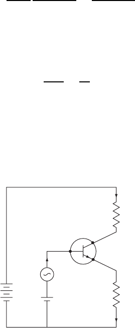
A simplified circuit illustrating the use of an npn transistor as an amplifier of a
small ac voltage
vt is shown in Fig. W11.14. The dc voltage sources V
eb
and V
bc
provide the biasing of the two p-n junctions and the source of the input signal vt
is placed in the base circuit. Kirchhoff’s loop rule applied to the emitter–base circuit
can be written as
V
bc
C vt D V
b
V
e
I
e
R
e
.W11.36
Since the emitter–base junction is forward-biased, the voltage drop V
b
V
e
across
the n-p junction will in general be much smaller than the other terms in this equation.
Therefore, Eq. (W11.35) can be rewritten with the help of Eq. (W11.36) as
I
c
D
ˇ
1 C ˇ
V
bc
C vt
R
e
³
V
bc
C vt
R
e
.W11.37
The additional output voltage V
c
t appearing across the resistor R
c
in the collector
circuit and due to the input voltage
vt is equal to [I
c
v I
c
v D 0]R
c
.Thevoltage
gain of this transistor can therefore be shown to be
G D
V
c
jvj
D
R
c
R
e
.W11.38
Thus a small ac voltage in the base circuit can result in a much larger voltage in the
collector circuit. Typical voltage gains of junction transistors are ³ 100. In addition to
being used as an amplifier, transistors can also function as switches. In this case, by
controlling the base current I
b
using the base voltage, the much larger collector current
I
c
can be switched from a very high value to a very low value.
V
bc
V
b
I
b
I
c
I
e
R
e
R
c
V
c
V
e
V
eb
+
−
+
−
v(t)
Figure W11.14. Simplified circuit illustrating the use of an npn transistor as an amplifier of
a small ac voltage
vt. The dc voltage sources V
bc
and V
eb
provide the biasing of the two
junctions and the source of the input signal
vt appears in the base circuit.

126 SEMICONDUCTORS
The intrinsic switching speed of the npn junction transistor described here is limited
by the time it takes the minority-carrier electrons to travel across the base region of
thickness d. Since the distance traveled by a diffusing electron in time t is given by
d D
p
Dt,whereD is the electron’s diffusivity, the electron transit time or switching
time of the transistor is
t
tr
¾
D
d
2
D
D
ed
2
e
k
B
T
.W11.39
Here
e
is the mobility of the minority-carrier electrons, and the Einstein relation
given for D in Eq. (11.81) has been used. To achieve high switching speeds and
operation at high frequencies (i.e., a rapid response of the transistor to changes in
applied signals), it is important to make the base region as thin as possible and also to
fabricate the transistor from a semiconductor with as high a mobility as possible. With
D ³ 5 ð 10
3
m
2
/s for Si and d ³ 1 µm, the value of t
tr
is ³ 2 ð10
10
s, while for
GaAs, values of t
tr
can be as low as 4 ð 10
11
s for the same value of d due to its
much higher diffusivity D ³ 0.023 m
2
/s. When the transit time t
tr
is shorter than the
minority-carrier lifetime (, the minority carriers can travel across the base ballistically
(i.e., without being scattered). Ballistic propagation of charge carriers can occur in a
device as its dimensions shrink in size and, as a result, the usual concepts of average
scattering time h(i and mobility D eh(i/m
Ł
c
play much less important roles in limiting
the drift velocities of the carriers and operation of the device. Under these conditions
very high device speeds can be achieved.
Transistor action in a bipolar npn junction transistor thus corresponds to the injection
of minority-carrier electrons across the forward-biased emitter–base n-p junction into
the p-type base region. These electrons diffuse across the base and then drift and diffuse
in the accelerating electric field of the reverse-biased base–collector p-n junction,
where they then appear as collector current. The base current I
b
, which limits the
current gain ˇ D I
c
/I
b
, corresponds to the back injection of holes from the base to
the emitter across the emitter–base n-p junction. The analysis of the operation of
a transistor must take into account the exact spatial distributions of dopants in the
emitter, base, and collector regions and must include the possible effects of high-level
injection.
A type of bipolar transistor that provides better gain and higher-frequency operation
than the bipolar junction transistor just discussed is the heterojunction bipolar transistor
(HBT). In an npn HBT the emitter is an n-type semiconductor with a wider bandgap
than the base and collector semiconductors. The electron energy-band diagram for an
HBT shown in Fig. W11.15 indicates that a potential barrier exists in the valence band
which hinders the back injection of holes from the p-type base into the emitter, thereby
limiting the current I
b
flowing in the base circuit and increasing the current gain ˇ D
I
c
/I
b
. Due to the very fast, ballistic transport across the base, in contrast to the slower
diffusive transport that is ordinarily observed in bipolar junction transistors, HBTs
have been developed into the fastest devices of this kind and are used in microwave
applications and wireless communication devices.
In one successful HBT structure composed of group III–V semiconductors, InP
with E
g
D 1.27 eV is grown epitaxially on a lattice-matched In
0.53
Ga
0.47
As alloy
with E
g
³ 0.8 eV. Electrons from the InP emitter reach the heavily doped p
C
-type
In
0.53
Ga
0.47
As base region with excess kinetic energy and travel essentially ballisti-
cally to the collector. The high cutoff frequency of 165 GHz and average electron
SEMICONDUCTORS 127
Distance
e
−
CB
min
E
Fh
V
CB
E
Fe
Z
B
Z
C
Emitter Base
Collector depletion
region
Subcollector
Energy
Φ
BC
Figure W11.15. Electron energy-band diagram for a heterojunction bipolar transistor (HBT).
In the npn HBT shown here the emitter has a wider bandgap than the base and collector
semiconductors. A potential barrier exists in the valence band that hinders the back injection of
holes from the p-type base into the emitter. (From A. F. J. Levi et al., Phys. Today, Feb. 1990,
p. 61. Copyright
1990 by the American Institute of Physics.)
velocity of 4 ð 10
5
m/s measured at T D 300 K in the active region correspond to a
total delay of less than 1 ps in the active region between the emitter and the bulk
of the collector. The extreme process control ideally required for the fabrication of
such HBT devices is indicated by the need to maintain an atomically flat interface
between the InP emitter and the base and to restrict the width of the emitter–base
doping profile to about 5 nm. Molecular beam epitaxy, described in Chapter W21, is
capable of achieving the control needed in the deposition process. Nevertheless, due
to the extreme deposition control needed and due to the lack of a reliable native oxide,
these group III–V-based devices are unlikely to replace Si technology, despite their
outstanding characteristics.
Another material demonstrating impressive performance and high speed in HBT
structures is alloys of SiGe grown heteroepitaxially on Si substrates. The lower-bandgap
p-type SiGe base region in Si–SiGe HBTs allows carriers to travel much faster across
the base and thus operation at higher frequencies.
A class of transistors whose operation involves only majority carriers is known as
field-effect transistors (FETs). These devices are simpler than bipolar junction tran-
sistors and correspond in practice to a resistor whose resistance is controlled by an
applied voltage and the resulting electric field in the semiconductor. They therefore
operate on a completely different physical mechanism than the bipolar junction tran-
sistors. Instead of having an emitter, collector, and base, FETs consist of a source and
a drain for electrons and a gate that is used either to control or create a conducting
channel in the semiconductor. FETs can be viewed as electronic switches that are in
either an “on” or an “off” state. As a result, an FET corresponds in a real sense to
a single bit (i.e., a binary unit of information). The junction field-effect transistor is
discussed briefly next. The metal–oxide–semiconductor FET (MOSFET) is described
in Chapter 11.

128 SEMICONDUCTORS
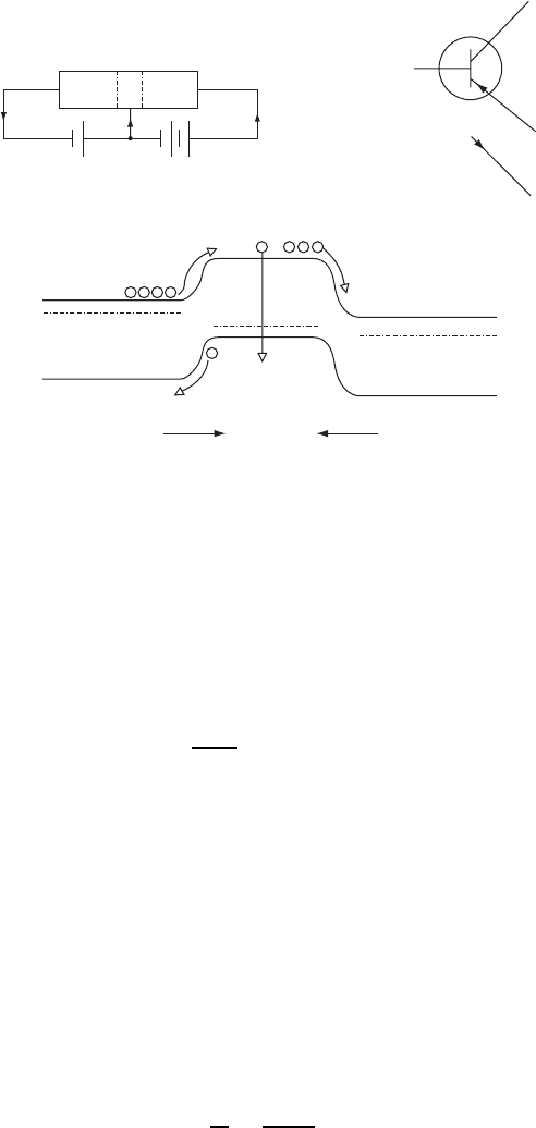
Junction Field-Effect Transistor. The configuration of a junction FET in a rect-
angular bar of n-type Si is shown schematically in Fig. W11.16. The two metallic
electrodes at the ends of the bar are the source and drain and the conducting channel
in the n-type Si between them is controlled by the two p
C
-type gates at the center
of the bar. The bar of Si acts as a resistor whose resistance R is controlled by the
reverse-bias gate voltage V
g
.AsV
g
is increased, the depletion regions at the two
reverse-biased p
C
-n junctions widen and effectively restrict the cross-sectional area
of the path or conducting channel of the majority-carrier electrons as they flow from
source to drain. The conductance G D 1/R of the Si bar is therefore controlled by the
gate voltage V
g
. The junction FET is “on” when the channel is open and conducting
and is “off” when it is closed and nonconducting. The speed of the junction FET is
controlled by the transit time of the majority carriers through the channel and so is
inversely proportional to the gate length.
Current–voltage characteristics of a junction FET are also presented in Fig. W11.16
in the form of the source-to-drain current I
d
versus the source-to-drain voltage V
d
for
a series of gate voltages V
g
.ForagivenV
g
, the current I
d
is observed to increase
linearly and then to saturate. The analysis of the current response of a junction FET is
complicated by the fact that the widths of the two depletion regions on opposite sides
of the bar are not constant along the channel. As shown in Fig. W11.16, the width
will be greater near the drain, where the voltage V
d
adds its contribution to the reverse
biasing of the two p
C
-n junctions. The conducting channel will be “pinched” (i.e., will
decrease in cross-sectional area to a small value) when the two depletion regions are
very close to each other near the drain electrode. The current I
d
does not in fact go to
zero due to this “pinching” effect but instead, saturates, as observed. As the channel
shrinks in cross section, the electric field lines are squeezed into a smaller area. As a
result, the electric field in the channel increases and current continues to flow. In this
case, Ohm’s law will no longer be valid when the electric field reaches a value where
the mobility of the majority carriers starts to decrease due to inelastic scattering effects
associated with “hot” carriers, as described in the discussion of high-field effects in
Section 11.7.
The rapid increase in drain current I
d
that is observed to occur in Fig. W11.16 as
either V
g
and/or V
d
increase in magnitude is just the junction breakdown which occurs
when the p
C
-n junctions are strongly reverse-biased. It can be seen that both V
g
and
V
d
contribute to the breakdown of the junction FET.
In the junction FET the gate voltage effectively controls the resistance R or conduc-
tance G of the p-type Si region and so controls the flow of current through the device.
The transconductance of the transistor is defined by
g
m
D
∂I
d
∂V
g
.W11.40
Here g
m
expresses the degree of amplification and control of the source-to-drain current
I
d
by the gate voltage V
g
and is one of the most important characteristics of the
transistor.
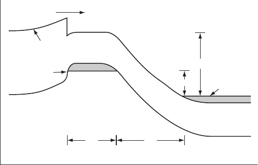
Other Types of Transistors. An intrinsic problem in semiconductor devices is
that the doping procedure which provides the majority carriers can also lead to a
decrease in the carrier mobility at high doping levels, as illustrated in Fig. 11.15. This