Gersten J.I., Smith F.W. The Physics and Chemistry of Materials
Подождите немного. Документ загружается.

SEMICONDUCTORS 109
transferred by the electron as it moves through the semiconductor, with a ³ 1.5to
2, depending on the dominant scattering process. Therefore, the net heat flow due to
electrons is from left to right through the semiconductor, with the temperature gradient
in the direction shown. It follows in this case for electrons that the magnitude of the
Peltier coefficient (i.e., the net energy transported by each electron divided by the
charge e)is
n
T D TS
n
T D
E
c
C ak
B
T
e
.W11.17
This result is consistent with Eq. (W11.15). Note that the position of the chemical
potential within the energy gap can be determined from a measurement of
n
as
T ! 0K.
For the p-type semiconductor shown in Fig. W11.4, holes will flow from right to
left. Since the energy of a hole increases in the downward direction on this electron
energy scale, only the most energetic holes can pass into the semiconductor over the
energy barrier E
v
at the junction on the right. In this case the net heat flow is
from right to left, with the temperature gradient in the direction shown. It follows for
holes that
p
T D TS
p
T D
E
v
C ak
B
T
e
,W11.18
which is consistent with Eq. (W11.16).
The contribution of phonons to the thermoelectric power originates in the phonon
drag effect, the tendency of phonons diffusing from the hot to the cold end of a
material to transfer momentum to the electrons, thereby “dragging” them along in the
same direction. This effect becomes more noticeable at lower temperatures.
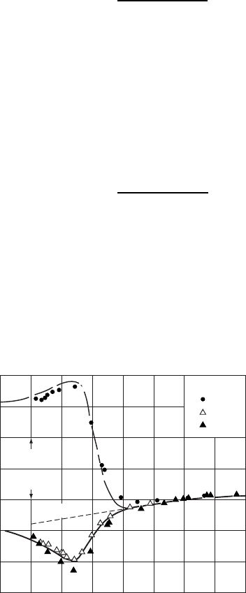
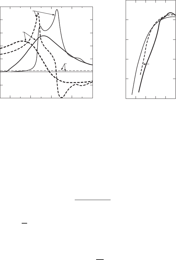
Experimental results and theoretical predictions for the Peltier coefficient for n-
and p-type Si as functions of temperature are shown in Fig. W11.5. The Si samples
×
×
×
×
×
×
×
×
×
200
−0.8
−0.6
−0.4
−0.2
0
0.2
0.4
0.6
300 400 500 600 700 800 900 1000
Π = TS (V)
T (K)
p
-type
(Intrinsic)
n
-type
p
-type
n
-type
Figure W11.5. Experimental results (points) and theoretical predictions (solid lines) for the
Peltier coefficient for n-andp-type Si are shown as functions of temperature. The Si
samples show intrinsic behavior above T ³ 600 K. (From T. H. Geballe et al., Phys. Rev., 98,
940 (1955). Copyright
1955 by the American Physical Society.)

110 SEMICONDUCTORS
show intrinsic behavior above T ³ 600 K. Note that plots of e versus T yield as
intercepts at T D 0 K, the quantities E
c
and ( E
v
)forn-andp-type semi-
conductors, respectively. This is a convenient way of determining the position of the
chemical potential relative to the band edges in doped semiconductors.
W11.5 Dielectric Model for Bonding
In the dielectric model of Phillips and Van Vechten (PV) for tetrahedrally coordi-
nated semiconductors with diamond and zincblende crystal structures the chemical
bonding is considered to be the sum of covalent and ionic contributions. As discussed
in Section 2.6, f
c
is the fraction of covalent bonding in an A–B bond involving atoms
A and B, while the ionic fraction or ionicity is f
i
D 1 f
c
.Valuesoff
i
obtained on
the basis of the PV model are presented in Table 2.6. These values are based on the
dielectric properties of these materials and differ somewhat from those proposed by
Pauling, which are based on the thermochemistry of solids.
In the PV model the average total energy gap E
g
(A–B) in, for example, a binary
compound AB containing only A–B bonds is defined as the average energy separa-
tion between the bonding and antibonding energy levels associated with the orbitals
involved in the A–B bond. Thus E
g
is not an observable quantity and is in some sense
an average energy gap between the valence and conduction bands. A spectroscopic
or dielectric definition for E
g
is used in the PV model rather than a thermochemical
definition based on heats of formation or cohesive energies. Specifically, E
g
(A-B) is
defined experimentally in terms of the measured optical dielectric function by
/0
/
o
D 1 CA
1
¯hω
p
E
g
2
,W11.19
where
ω
2
p
D
ne
2
m/
o
.
Here /0//
o
D n
2
(0) is the real, zero-frequency limit of the complex dielectric function
/ω, q//
o
, also known as the relative permittivity /
r
,andω
p
is the plasma frequency.
Also, n is the concentration of valence electrons, /
o
the permittivity of free space, and
A
1
a correction factor that is close to 1 which accounts for the possible participation
of d electrons in the optical response. The bonding–antibonding energy gap E
g
(A–B)
differs from and is typically much larger than the optical energy gap E
g
D E
c
E
v
.
Equation (W11.19) is close in form to the expression given in Eq. (8.32), which is
derived from the Lorentz oscillator model for the optical dielectric function.
When the A–B bond is of a mixed ionic–covalent type, the gap E
g
(A–B) is taken
to be complex, with a real covalent or homopolar component E
h
andanimaginary
ionic or heteropolar component iC,sothat
E
g
A–B D E
h
C iC,
jE
g
j
2
D E
2
h
C C
2
.
W11.20
SEMICONDUCTORS 111
The definitions of E
h
and C in terms of microscopic parameters associated with the
A–B bond and the binary AB compound are
E
h
A–B D
A
2
d
2.5
,
CA–B D 14.4b
z
A
r
A
z
B
r
B
exp
k
TF
d
2
.
W11.21
where A
2
D 39.74 eV, the dimensionless constant b ³ 1.5, d is the A–B interatomic
distance or bond length, and z
A
and z
B
are the valences and r
A
and r
B
the covalent
radii of atoms A and B, respectively, with d D r
A
C r
B
.HereE
h
and C are given in
eV when r
A
and r
B
are in angstrom units. The exponential Thomas–Fermi screening
factor, defined in Section 7.17, describes the screening of the ion cores by the valence
electrons and is expressed in terms of the Thomas–Fermi wave vector or inverse
screening length:
k
TF
D
3ne
2
2/E
F
D
e
2
E
F
/
,W11.22
where n is the concentration of valence electrons, E
F
the Fermi energy, / the permit-
tivity of the material, and E
F
the electron density of states per unit volume. Typical
values of k
TF
are ³ 5 ð 10
10
m
1
. It can be seen that C(A–B) is given by the difference
between the Coulomb potentials of the two atoms A and B composing the bond.
The use of known values of d(A–A) and of E
g
(A–A) determined from /(0) using
Eq. (W11.19) for the covalent elemental semiconductors diamond and Si allows both
the exponent of d, 2.5, and the constant A
2
D 39.74 eV to be determined in the
expression for E
h
. The ionic component C(A–B) of E
g
(A–B) for binary AB semi-
conductors can then be calculated using Eq. (W11.20) from empirical values of E
g
determined from Eq. (W11.19) and values of E
h
(A–B) calculated from Eq. (W11.21).
It has been shown empirically that the ionic contribution CA–B / X
A
X
B
,the
difference of the electronegativities of the two atoms.
The ionicity of the A–B bond is defined in a straightforward manner by
f
i
D
C
2
E
g
2
.W11.23
Thus f
i
D 0whenC D 0andf
i
! 1forC × E
h
. The ionicities presented in
Table 2.6, known as spectroscopic ionicities, have been calculated in this way using
the PV model. For group III–V compounds it has been found that C is usually smaller
than E
h
so that f
i
< 0.5. The bonding in these compounds is therefore predominantly
covalent. The reverse is true for the group II–VI and I–VII compounds, where C is
usually greater than E
h
.
Va l ue s of E
h
, C, E
g
A B,andf
i
for several semiconductors with the diamond
or zincblende crystal structures are presented in Table W11.1. Note that E
h
is nearly
constant for isoelectronic sequences (e.g., for Ge, GaAs, and ZnSe), where E
h
³
4.3 eV, since their NN distances d are nearly constant. The optical energy gap E
g
and the average total energy gap E
g
(A–B) are neither proportional to nor simply
112 SEMICONDUCTORS
TABLE W11.1 Values of E
h
, C , E
g
.A − B /,andf
i
for Several Semiconductors
Semiconductor
IV III–V II–VI E
h
(eV) C (eV) E
g
A B (eV) f
i
E
g
/E
g
(A–B)
C (diamond) 13.5 0 13.5 0 0.40
BN 13.1 7.71 15.2 0.256 0.39
BeO 11.5 13.9 18.0 0.602 0.52
3C–SiC (ˇ-SiC) 8.27 3.85 9.12 0.177 0.25
Si 4.77 0 4.77 0 0.23
AlP 4.72 3.14 5.67 0.307 0.43
MgS 3.71 7.10 8.01 0.786 0.55
Ge 4.31 0 4.31 0 0.16
GaAs 4.32 2.90 5.20 0.310 0.26
ZnSe 4.29 5.60 7.05 0.630 0.37
Gray Sn 3.06 0 3.06 0 0.026
InSb 3.08 2.10 3.73 0.321 0.028
CdTe 3.08 4.90 5.79 0.717 0.25
related to each other [e.g., for the group IV elements, the ratio E
g
/E
g
(A–B) decreases
from 0.4 for diamond to 0.026 for gray Sn].
A test of the usefulness of this definition of ionicity has been provided by correlating
f
i
with the crystal structures of about 70 binary group IV–IV, III–V, II–VI, and I–VII
compounds. It is found that compounds with f
i
<f
ic
D 0.785 are all tetrahedrally
coordinated and semiconducting with either the diamond, zincblende, or wurtzite crystal
structures, while those with f
i
> 0.785 are all octahedrally coordinated and insulating
with the higher-density NaCl crystal structure. This is an impressive confirmation of
the usefulness of the definition of ionicity provided by the PV model.
A definition of electronegativity has also been formulated in the PV model for
nontransition metal elements with tetrahedral coordination. This definition differs from
that of Pauling presented in Section 2.9 by including the screening of the ion cores
by the valence electrons and is likely to be a more useful definition for this group of
elements and crystal structures.
W11.6 Nonstandard Semiconductors
In addition to the standard semiconductors discussed in our textbook, which typically
have the diamond, zincblende, wurtzite, or NaCl crystal structures, there also exist
nonstandard semiconducting materials with a variety of other structures and properties,
including disordered or amorphous semiconductors, oxide, organic, and magnetic semi-
conductors, and porous Si. Some interesting and technologically important examples
of these semiconductors are next discussed briefly.
Amorphous Semiconductors. Amorphous semiconductors that lack the long-range
order found in their crystalline counterparts often retain to a first approximation the
short-range order corresponding to the NN local bonding configurations present in
the crystal. For example, in amorphous Si (a-Si) essentially every Si atom is bonded
to four NN Si atoms in a nearly tetrahedral arrangement, with bond lengths close
to the crystalline value but with a significant spread of bond angles, ³ 7
o
, centered
SEMICONDUCTORS 113
around the ideal value of 109.47
o
. As a result, a-Si and crystalline Si (c-Si) are similar
in many respects, including atomic density and the fact that both are semiconduc-
tors with similar energy gaps. They differ appreciably in other important respects,
including carrier mobility and ease of doping. The most important defects in a-Si
correspond to broken or dangling bonds that are likely to be associated with voids in
the material and that give rise to electronic levels lying deep within the energy gap.
In addition, distorted or weak Si–Si bonds can give rise to electronic states, referred
to as tail states, that are localized in space and that lie within the energy gap near the
band edges.
The electron densities of states of c-Si, a-Si, and a-Si:H in and near the energy gap
are shown schematically in Fig. W11.6. The density of states for c-Si has sharp edges
at E D E
v
and at E D E
c
. While the densities of states for the amorphous case are
very material dependent, there exists a strong similarity between the overall shapes of
the curves except in the gap region itself. The dangling-bond defect states in a-Si pin
the Fermi energy E
F
, thereby preventing its movement in the gap. These defect states
thus interfere with the doping of this material and consequently with its electronic
applications.
The optical dielectric functions of c-Si and a-Si are compared in Fig. W11.7a.
The optical response in the crystalline and amorphous phases is qualitatively the same,
especially at low energies where /
1
0 D n
2
0 is essentially the same since the atomic
density of the sample of a-Si is only slightly less than that of c-Si. At higher energies
it can be seen that the structure in /
1
and /
2
observed in c-Si which is related to the
existence of long-range order is absent in the amorphous material where k conservation
is no longer required. The value of the optical energy gap E
opt
in amorphous semicon-
ductors such as a-Si and a-Si:H is often obtained using the Tauc law for band-to-band
E
v
E
v
E
v
ρ(E)
ρ(E)
E
c
E
c
E
c
E
0
0
0
1
1.8 eV
1.6 eV
1.1 eV
2
10
23
10
24
10
25
10
26
10
27
a-Si
c-Si
a-Si:H
10
23
10
24
10
25
10
26
10
27
10
23
10
24
10
25
10
26
10
27
ρ(E)
[eV
−1
m
−3
]
Figure W11.6. Electron densities of states in crystalline Si, a-Si, and a-Si:H in the region of
the energy gap.
114 SEMICONDUCTORS
0
−10
−20
10
20
30
40
50
324
(b)
E (eV)
hω (eV)
5
0
10
4
10
5
10
6
10
7
α
(m
−1
)
10
8
123 54
6
c-Si
a-Si
a-Si
c-Si
c-Si
a-Si
a-Si : H
Void
(a)
–
∋
1
∋
2
∋
Figure W11.7. Comparison of the optical properties of crystalline and amorphous Si. (a)The
quantities /
1
(dashed lines) and /
2
(solid lines) of c-Si and a-Si are plotted versus photon
energy E D ¯hω. (From B. G. Bagley et al., in B. R. Appleton and G. K. Celler, eds., Laser and
Electron-Beam Interactions with Solids, Copyright 1982, with permission from Elsevier Science).
(b) The logarithm of the optical absorption coefficient ˛ is plotted as a function of photon energy
¯hω for c-Si, a-Si, and a-Si:H. (Data from E. D. Palik, Handbook of Optical Constants of Solids,
Vol. 1, Academic Press, San Diego, Calif., 1985.)
absorption:
/
2
ω D
B¯hω E
opt
2
¯hω
2
,W11.24
where B is a constant and E
opt
³ E
c
E
v
. The parameter E
opt
can therefore be obtained
from a plot of ¯hω
p
/
2
versus ¯hω. Absorption at lower energies involving the tail states at
either the valence- or conduction-band edges is often observed to depend exponentially
on ¯hω, according to the Urbach edge expression:
˛ω D ˛
o
exp
¯hω
E
o
.W11.25
Here E
o
is the Urbach edge parameter and is related to the width of the tail-state regions,
while ˛
o
is a constant. In high-quality a-Si:H films, E
o
can be as low as 0.05 eV.
Even though the optical energy gap is larger for a-Si, ³ 1.6 eV, than for c-Si, light
is still absorbed in a-Si for energies below 1.6 eV. In fact, as shown in Fig. W11.7b,
both a-Si and a-Si:H have much higher absorption coefficients than c-Si in the region
of the visible spectrum up to 3 eV, at which point direct transitions begin in c-Si. This
is due in part to the fact that in c-Si the absorption corresponds to indirect transitions
for energies below 3 eV and also to the fact that absorption in a-Si can occur below the
optical gap due to transitions from localized to extended states, and vice versa. Thus
films of a-Si:H in photovoltaic solar cells with thicknesses ³ 1
µm are thick enough
SEMICONDUCTORS 115
to absorb most of the solar spectrum, while much thicker films of c-Si are required for
the same purpose.
In a-Si and other amorphous semiconductors such as a-Ge there exist mobility edges
located at E
v
and E
c
, respectively, as shown in Fig. W11.6. These mobility edges for
charge carriers typically lie in the tail-state regions and divide electron states in the gap
which are spatially localized from those in the energy bands that extend throughout
the material. The corresponding charge-carrier mobilities
e
and
h
are essentially
zero within the gap and are finite for E<E
v
and E>E
c
within the bands. Thermally
activated conduction of charge can still occur within the localized states in the gap
and at low temperatures will take place via variable-range hopping, as described in
Chapter 7.
Hydrogenated amorphous Si (a-Si:H) is a particularly useful alloy in which the
incorporation of H atoms leads to the removal of localized defect states from the energy
gap of a-Si by forming Si–H bonds with most of the Si atoms which otherwise would
have dangling bonds. The tail states associated with weak Si–Si bonds in a-Si can also
be eliminated via the formation of pairs of strong Si–H bonds. The electrons occupying
the strong Si–H bonds have energy levels lying within the valence band of the material,
well below the band edge at E
v
. In this way the concentration of electrically active
defects can be reduced from ³ 10
26
eV
1
m
3
in a-Si (about one active defect per
10
3
Si atoms) to ³ 10
21
eV
1
m
3
in a-Si:H (one active defect per 10
8
Si atoms). The
density of states in a-Si:H resulting from the incorporation of hydrogen is also shown
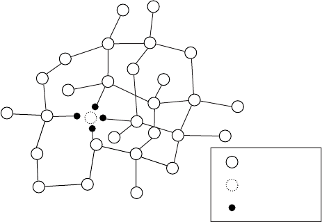
in Fig. W11.6. A schematic model of a segment of the continuous random network
(CRN) corresponding to the bonding in a-Si:H is shown in Fig. W11.8. Four H atoms
are shown completing the Si bonds at a Si monovacancy. This is an example of the
type of three-dimensional CRN structure discussed in Chapter 4. Films of a-Si:H are
typically formed by plasma deposition from the vapor phase onto substrates usually
held at T ³ 250
°
C.
The a-Si:H alloys can be successfully doped n-orp-type during deposition using
the standard dopant atoms P and B and as a result have found important applications
in photovoltaic solar cells and in the thin-film transistors (TFTs) used as switching
elements in flat panel displays. These applications are described in Sections W11.8 and
v
Si atom
Si vacancy
H atom
v
Figure W11.8. Model of a segment of the continuous random network corresponding to the
bonding in a-Si:H. Four H atoms are shown completing the Si bonds at a Si monovacancy.
116 SEMICONDUCTORS
W11.10. The extended-state carrier mobilities in a-Si:H,
e
³ 10
4
to 10
3
m
2
/VÐsand
h
³ 3 ð10
7
m
2
/VÐs, are well below those found in crystalline Si,
e
³ 0.19 m
2
/VÐs,
due to the disorder and increased scattering present in the amorphous material. The
electrical conductivities attainable in a-Si:H by doping,
n
³ 1
1
m
1
and
p
³
10
2
1
m
1
, are also well below those readily attainable in c-Si, ³ 10
4
1
m
1
.
In amorphous alloys based on Si, C, and H, the optical gap can be varied from
E
g
³ 1.8 eV for a-Si:H to above 3 eV for a-Si
0.5
C
0.5
:H, thus making the latter material
useful as a “window” layer in photovoltaic solar cells. The attainment of even larger
gaps at higher C contents is limited by the tendency in carbon-rich alloys for a mixture
of tetrahedral (i.e., diamond-like) and trigonal (i.e., graphite-like) bonding of the C
atoms to be present. The amorphous graphitic component of hydrogenated amorphous
carbon, a-C:H, has an energy gap E
g
³ 0.5eV.
Amorphous semiconducting chalcogenide-based glasses such as a-Se and a-As
2
S
3
have both covalent and van der Waals components in their chemical bonding, as
discussed in Section 2.2. These amorphous materials can contain molecular units such
as (Se)
8
and therefore have networks of lower dimensionality and greater structural
flexibility than a-Si and a-Ge in which the bonding is three-dimensional. A schematic
model of the essentially two-dimensional CRN of a-As
2
S
3
and other related mate-
rials is shown in Fig. 4.12. In these chalcogenide glasses, group V elements such as
As are threefold coordinated and group VI elements such as S and Se are twofold
coordinated, as in the crystalline counterparts. The highest-filled valence band in these
materials typically consists of electrons occupying lone-pair orbitals on the chalco-
genide atoms rather than electrons participating in chemical bonds with their NNs.
These glasses are typically formed by rapid quenching from the liquid phase. Appli-
cations of amorphous chalcogenide-based glasses include their use in xerography as
photoconductors, as described in Chapter 18.
Oxide Semiconductors. Some well-known oxide semiconductors include Cu
2
O
(cuprite), CuO, and CuO
2
. Some group III–V compounds which include oxygen as
the group V element are listed in Table 11.9. Semiconducting oxides such as SnO
2
,
In
2
O
3
, ITO (indium–tin oxide), Cd
2
SnO
4
, and ZnO can be prepared as transparent,
conducting coatings and have found a wide range of applications (e.g., as transparent
electrodes for photovoltaic solar cells).
Copper-based oxides such as La
2
CuO
4
with E
g
³ 2.2 eV and with the perovskite
crystal structure have received considerable attention recently due to the discovery of
the high-T
c
superconductivity that is observed when they become metallic through
doping or alloying. For example, when La
2
CuO
4
becomes p-type through the replace-
ment of La
3C
by Sr
2C
, the resulting material La
2x
Sr
x
CuO
4
is metallic for x>0.06
and becomes superconducting at low temperatures, as described in Chapter 16.
Organic Semiconductors. Conjugated organic materials such as polymers
possessing resonant ,-electron bonding can be classified as semiconductors when the
energy gap E
g
associated with the ,-electron system is in the range 1 to 3 eV. The
one-dimensional polymer polyacetylene, (CH)
n
, with alternating single and double
carbon–carbon bonds, can possess very high electrical conductivities, exceeding that
of copper, when suitable n-type (Na or Hg) or p-type (I) dopants are introduced. Other
polymers, such as polypyrrole and polyaniline, can also exhibit high conductivities
when suitably doped. A detailed description of the electronic structure and doping of
SEMICONDUCTORS 117
polyacetylene is presented in Chapter W14. The large nonlinear optical effects found
in these materials may lead to important optoelectronic applications. Other applications
include their use as photoconductors in xerography.
Semiconducting organic molecular crystals can also exhibit strong electrolumines-
cence and photoluminescence and thus have potential applications in organic light-
emitting diodes.
Magnetic Semiconductors. Wide-bandgap ZnS and CdTe and narrow-bandgap
HgTe group II–VI semiconductors when alloyed with magnetic impurities such as
Mn (e.g., Zn
1x
Mn
x
S with 0 x 0.5) have potentially important applications based
in part on the “giant” Faraday rotations and negative magnetoresistances which they
can exhibit. The sp–d exchange interaction between the s and p conduction-band elec-
trons and the d electrons of the magnetic ions leads to very large Zeeman splittings at
the absorption edge and also of the free-exciton level. This sp–d interaction provides
the mechanism for the Faraday rotation observed for light propagating in the direction
of an applied magnetic field. The magnetic properties of these materials, known as
dilute magnetic semiconductors, are discussed briefly in Chapter W17.
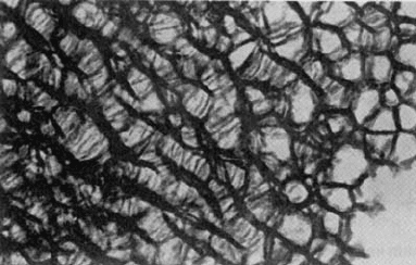
Porous Si. An interesting form of Si that may have useful light-emitting applications
is porous Si, prepared via electrochemical etching of the surfaces of Si wafers. Porous
Si is believed to be a network composed of nanometer-sized regions of crystalline
Si surrounded by voids which can occupy between 50 to 90% of the volume of the
material. A transmission electron micrograph of porous Si in which the Si columns
are about 10 nm in diameter and the pore spaces are about 50 nm wide is shown
in Fig. W11.9. Tunable room-temperature photoluminescence in porous Si has been
achieved from the near-infrared to the blue-green region of the visible spectrum.
Proposals for the origins of the light emission from porous Si have focused on the
quantum confinement of charge carriers in Si regions with dimensions of 2 to 3 nm.
Other possible explanations are that oxidized regions with their larger bandgaps or the
effects of impurities such as hydrogen can explain the emission of light. It seems clear
in any case that oxygen and hydrogen play important roles in chemically passivating
the surfaces of the Si nanocrystals. These surfaces would otherwise provide surface
recombination sites that would quench the observed luminescence.
Figure W11.9. Transmission electron micrograph of porous Si in which the Si columns are
about 10 nm in diameter and the pore spaces are about 50 nm wide. (Reprinted with permission
of A. G. Cullis. From R. T. Collins et al., Phys. Today, Jan. 1997, p. 26.)
118 SEMICONDUCTORS
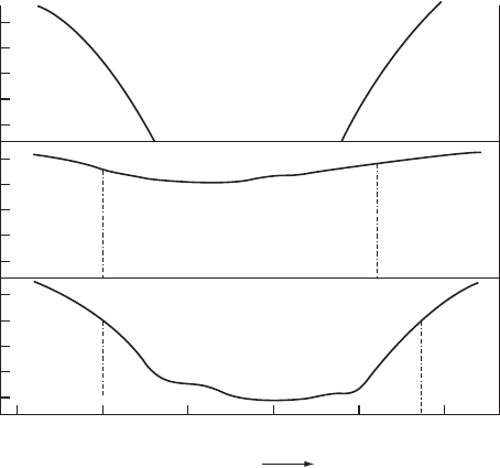
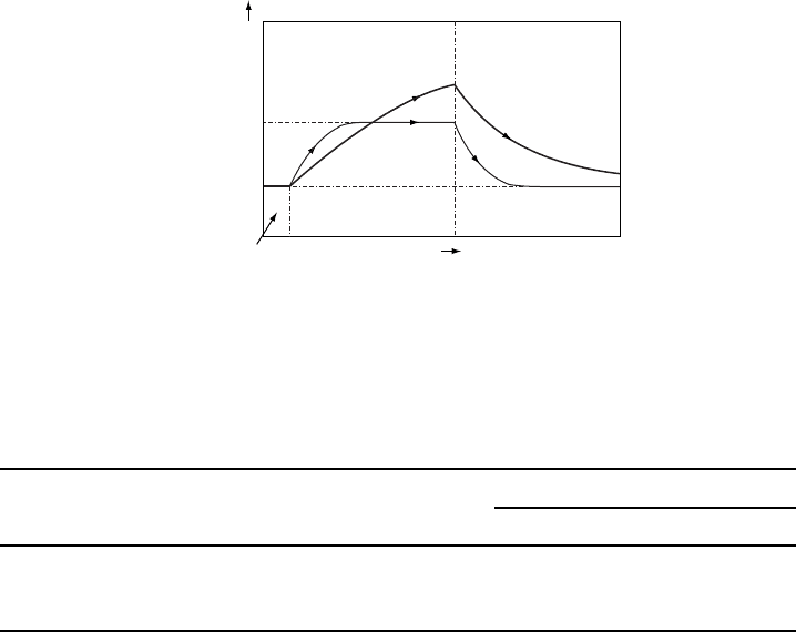
W11.7 Further Discussion of Nonequilibrium Effects and Recombination
The buildup and decay of p
n
t according to Eqs. (11.74) and (11.77), respectively,
are illustrated in Fig. W11.10. Band-to-band radiative recombination can be impor-
tant in highly perfect crystals of direct-bandgap semiconductors such as GaAs but is
very unlikely to be important in Si, Ge, and GaP. Indirect-bandgap semiconductors
have much longer recombination times (i.e., minority-carrier radiative lifetimes) than
direct-bandgap materials as a result of the requirement that a phonon participate in
the band-to-band recombination process. Some calculated values for minority-carrier
band-to-band radiative lifetimes are given in Table W11.2. These lifetimes have been
calculated using the van Roosbroeck–Shockley relation andarebasedonmeasured
optical properties (i.e., the absorption coefficient ˛ andindexofrefractionn), and on
the carrier concentrations of these semiconductors. The van Roosbroeck–Shockley
relation expresses a fundamental connection between the absorption and emission
spectra of a semiconductor and allows calculation of the band-to-band recombina-
tion rate in terms of an integral over photon energy involving ˛ and n. Note that
the calculated intrinsic lifetimes span the range from hours for Si to microseconds
for InAs.
Measured values of (
p
and (
n
in semiconductors such as Si and GaAs are often much
lower than the calculated values because of enhanced recombination due to defects and
p
n
p
n
(t)
t
1
2
p
o
G
I
= 0
G
I
= 0
G
I
> 0
p
o
+G
I
τ
p
(1)
Figure W11.10. Buildup and decay of the minority-carrier hole concentration p
n
t in an n-type
semiconductor under low-level carrier injection for two different minority-carrier lifetimes, with
(
p
1<(
p
2.
TABLE W11.2 Calculated Minority-Carrier Band-to-Band Radiative Lifetimes at
T
= 300 K
Lifetime
Semiconductor n
i
(m
3
) Intrinsic
a
Extrinsic
b
Si ³8 ð 10
15
4.6 h 2.5 ms
Ge ³2 ð 10
19
0.61 s 0.15 ms
InAs ³2 ð10
21
15 µs0.24µs
a
Lifetimes are calculated values obtained from R. N. Hall, Proc. Inst. Electr. Eng., 106B, Suppl. 17, 923
(1959).
b
The extrinsic lifetimes correspond to carrier concentrations of 10
23
m
3
.