Fuller S.H., Millett L.I. The Future of Computing Performance: Game Over or Next Level?
Подождите немного. Документ загружается.

Copyright © National Academy of Sciences. All rights reserved.
The Future of Computing Performance: Game Over or Next Level?
166 THE FUTURE OF COMPUTING PERFORMANCE
Kathryn S. McKinley is a professor at the University of Texas at Austin.
Her research interests include compilers, runtime systems, and architec-
ture. Her research seeks to enable high-level programming languages to
achieve high performance, reliability, and availability. She and her collab-
orators have developed compiler optimizations for improving memory-
system performance, high-performance garbage-collection algorithms,
scalable explicit-memory management algorithms for parallel systems,
and cooperative dynamic optimizations for improving the performance
of managed languages. She is leading the compiler effort for the TRIPS
project, which is exploring attaining scalable performance improvements
using explicit dataflow graph execution architectures. Her honors include
being named an Association for Computing Machinery (ACM) Distin-
guished Scientist and receiving a National Science Foundation Career
Award. She is the co-editor-in-chief of ACM’s Transactions on Programming
Language and Systems (TOPLAS). She is active in increasing minority-group
participation in computer science and, for example, co-led with Daniel
Jimenez the CRAW/CDC Programming Languages Summer School in
2007. She has published over 75 refereed articles and has supervised eight
PhD degrees. Dr. McKinley holds a BA (1985) in electrical engineering and
computer science and an MS (1990) and a PhD (1992) in computer science,
all from Rice University.
Charles Moore is an Advanced Micro Devices (AMD) corporate fellow and
the CTO for AMD’s Technology Group. He is the chief engineer of AMD’s
next-generation processor design. His responsibilities include interacting
with key customers to understand their requirements, identifying impor-
tant technology trends that may affect future designs, and architectural
development and management of the next-generation design. Before join-
ing AMD, Mr. Moore was a senior industrial research fellow at the Uni-
versity of Texas at Austin, where he did research on technology-scalable
computer architecture. Before then, he was a distinguished engineer at
IBM, where he was the chief engineer on the POWER4 project. Earlier, he
was the coleader of the first single-chip POWER architecture implementa-
tion and the coleader of the first PowerPC implementation used by Apple
Computer in its PowerMac line of personal computers. While at IBM, he
was elected to the IBM Academy of Technology and was named an IBM
master inventor. He has been granted 29 US patents and has several oth-
ers pending. He has published numerous conference papers and articles
on a wide array of subjects related to computer architecture and design.
He is on the editorial board of IEEE Micro magazine and on the program
committee for several important industry conferences. Mr. Moore holds a
master’s degree in electrical engineering from the University of Texas at
Copyright © National Academy of Sciences. All rights reserved.
The Future of Computing Performance: Game Over or Next Level?
APPENDIX B 167
Austin and a bachelor’s degree in electrical engineering from the Rens-
selaer Polytechnic Institute.
Katherine Yelick is a professor in the Computer Science Division of the
University of California, Berkeley. The main goal of her research is to
develop techniques for obtaining high performance on a wide array of
computational platforms and to ease the programming effort required to
obtain performance. Dr. Yelick is perhaps best known for her efforts in
global address space (GAS) languages, which attempt to present the pro-
grammer with a shared-memory model for parallel programming. Those
efforts have led to the design of Unified Parallel C (UPC), which merged
some of the ideas of three shared-address-space dialects of C: Split-C,
AC (from IDA), and PCP (from Lawrence Livermore National Labora-
tory). In recent years, UPC has gained recognition as an alternative to
message-passing programming for large-scale machines. Compaq, Sun,
Cray, HP, and SGI are implementing UPC, and she is currently leading a
large effort at Lawrence Berkeley National Laboratory to implement UPC
on Linux clusters and IBM machines and to develop new optimizations.
The language provides a uniform programming model for both shared
and distributed memory hardware. She has also worked on other global-
address-space languages, such as Titanium, which is based on Java. She
has done notable work on single-processor optimizations, including tech-
niques for automatically optimizing sparse matrix algorithms for memory
hierarchies. Another field that she has worked in is architectures for
memory-intensive applications and in particular the use of mixed logic,
which avoids the off-chip accesses to DRAM, thereby gaining bandwidth
while lowering latency and energy consumption. In the IRAM project, a
joint effort with David Patterson, she developed an architecture to take
advantage of this technology. The IRAM processor is a single-chip system
designed for low power and high performance in multimedia applica-
tions and achieves an estimated 6.4 gigaops per second in a 2-W design.
Dr. Yelick received her bachelor’s degree (1985), master’s degree (1985),
and PhD (1991) in electrical engineering and computer science from the
Massachusetts Institute of Technology.
STAFF
Lynette I. Millett is a senior program officer and study director at the
Computer Science and Telecommunications Board (CSTB), National
Research Council of the National Academies. She currently directs sev-
eral CSTB projects, including a study to advise the Centers for Medicare
and Medicaid Service on future information systems architectures and a
study examining opportunities for computing research to help meet sus-
Copyright © National Academy of Sciences. All rights reserved.
The Future of Computing Performance: Game Over or Next Level?
168 THE FUTURE OF COMPUTING PERFORMANCE
tainability challenges. She served as the study director for the CSTB report
Social Security Administration Electronic Service Provision: A Strategic Assess-
ment. Ms. Millett’s portfolio includes substantial portions of CSTB’s recent
work on software, identity systems, and privacy. She directed, among
other projects, those that produced Software for Dependable Systems: Suf-
ficient Evidence?, an exploration of fundamental approaches to develop-
ing dependable mission-critical systems; Biometric Recognition: Challenges
and Opportunities, a comprehensive assessment of biometric technology;
Who Goes There? Authentication Through the Lens of Privacy, a discussion of
authentication technologies and their privacy implications; and IDs—Not
That Easy: Questions About Nationwide Identity Systems, a post-9/11 analy-
sis of the challenges presented by large-scale identity systems. She has an
M.Sc. in computer science from Cornell University, where her work was
supported by graduate fellowships from the National Science Founda-
tion and the Intel Corporation; and a BA with honors in mathematics and
computer science from Colby College, where she was elected to Phi Beta
Kappa.
Shenae Bradley is a senior program assistant at the Computer Science
and Telecommunications Board of the National Research Council. She
currently provides support for the Committee on Sustaining Growth in
Computing Performance, the Committee on Wireless Technology Pros-
pects and Policy Options, and the Computational Thinking for Everyone:
A Workshop Series Planning Committee, to name a few. Prior to this, she
served as an administrative assistant for the Ironworker Management
Progressive Action Cooperative Trust and managed a number of apart-
ment rental communities for Edgewood Management Corporation in the
Maryland/DC/Delaware metropolitan areas. Ms. Bradley is in the pro-
cess of earning her BS in family studies from the University of Maryland
at College Park.
Copyright © National Academy of Sciences. All rights reserved.
The Future of Computing Performance: Game Over or Next Level?
C
Reprint of Gordon E. Moore’s
“Cramming More Components
onto Integrated Circuits”
NOTE: Reprinted from Gordon Moore, 1965, Cramming more components onto integrated
circuits, Electronics 38(8) with permission from Intel Corporation.
169

Copyright © National Academy of Sciences. All rights reserved.
The Future of Computing Performance: Game Over or Next Level?
170 THE FUTURE OF COMPUTING PERFORMANCE
Cramming More Components onto
Integrated Circuits
GORDON E. MOORE, LIFE FELLOW, IEEE
With unit cost falling as the number of components per circuit
rises, by 1975 economics may dictate squeezing as many as 65 000
components on a single silicon chip.
The future of integrated electronics is the future of
electronics itself. The advantages of integration will bring
about a proliferation of electronics, pushing this science
into many new areas.
Integrated circuits will lead to such wonders as home
computers—or at least terminals connected to a central
computer—automatic controls for automobiles, and per-
sonal portable communications equipment. The electronic
wristwatch needs only a display to be feasible today.
But the biggest potential lies in the production of large
systems. In telephone communications, integrated circuits
in digital lters will separate channels on multiplex equip-
ment. Integrated circuits will also switch telephone circuits
and perform data processing.
Computers will be more powerful, and will be organized
in completely different ways. For example, memories built
of integrated electronics may be distributed throughout
the machine instead of being concentrated in a central
unit. In addition, the improved reliability made possible
by integrated circuits will allow the construction of larger
processing units. Machines similar to those in existence
today will be built at lower costs and with faster turn-
around.
I. P
RESENT AND FUTURE
By integrated electronics, I mean all the various tech-
nologies which are referred to as microelectronics today
as well as any additional ones that result in electronics
functions supplied to the user as irreducible units. These
technologies were rst investigated in the late 1950’s. The
object was to miniaturize electronics equipment to include
increasingly complex electronic functions in limited space
with minimum weight. Several approaches evolved, includ-
ing microassembly techniques for individual components,
thin-lm structures, and semiconductor integrated circuits.
Reprinted from Gordon E. Moore, “Cramming More Components onto
Integrated Circuits,” Electronics, pp. 114–117, April 19, 1965.
Publisher Item Identier S 0018-9219(98)00753-1.
Each approach evolved rapidly and converged so that
each borrowed techniques from another. Many researchers
believe the way of the future to be a combination of the
various approaches.
The advocates of semiconductor integrated circuitry are
already using the improved characteristics of thin-lm
resistors by applying such lms directly to an active semi-
conductor substrate. Those advocating a technology based
upon lms are developing sophisticated techniques for the
attachment of active semiconductor devices to the passive
lm arrays.
Both approaches have worked well and are being used
in equipment today.
II. T
HE ESTABLISHMENT
Integrated electronics is established today. Its techniques
are almost mandatory for new military systems, since the
reliability, size, and weight required by some of them is
achievable only with integration. Such programs as Apollo,
for manned moon ight, have demonstrated the reliability
of integrated electronics by showing that complete circuit
functions are as free from failure as the best individual
transistors.
Most companies in the commercial computer eld have
machines in design or in early production employing inte-
grated electronics. These machines cost less and perform
better than those which use “conventional” electronics.
Instruments of various sorts, especially the rapidly in-
creasing numbers employing digital techniques, are starting
to use integration because it cuts costs of both manufacture
and design.
The use of linear integrated circuitry is still restricted
primarily to the military. Such integrated functions are ex-
pensive and not available in the variety required to satisfy a
major fraction of linear electronics. But the rst applications
are beginning to appear in commercial electronics, partic-
ularly in equipment which needs low-frequency ampliers
of small size.
III. R
ELIABILITY COUNTS
In almost every case, integrated electronics has demon-
strated high reliability. Even at the present level of pro-
82 PROCEEDINGS OF THE IEEE, VOL. 86, NO. 1, JANUARY 1998
Copyright © National Academy of Sciences. All rights reserved.
The Future of Computing Performance: Game Over or Next Level?
APPENDIX C 171
duction—low compared to that of discrete components—it
offers reduced systems cost, and in many systems improved
performance has been realized.
Integrated electronics will make electronic techniques
more generally available throughout all of society, perform-
ing many functions that presently are done inadequately by
other techniques or not done at all. The principal advantages
will be lower costs and greatly simplied design—payoffs
from a ready supply of low-cost functional packages.
For most applications, semiconductor integrated circuits
will predominate. Semiconductor devices are the only rea-
sonable candidates presently in existence for the active
elements of integrated circuits. Passive semiconductor el-
ements look attractive too, because of their potential for
low cost and high reliability, but they can be used only if
precision is not a prime requisite.
Silicon is likely to remain the basic material, although
others will be of use in specic applications. For example,
gallium arsenide will be important in integrated microwave
functions. But silicon will predominate at lower frequencies
because of the technology which has already evolved
around it and its oxide, and because it is an abundant and
relatively inexpensive starting material.
IV. C
OSTS AND CURVES
Reduced cost is one of the big attractions of integrated
electronics, and the cost advantage continues to increase
as the technology evolves toward the production of larger
and larger circuit functions on a single semiconductor
substrate. For simple circuits, the cost per component is
nearly inversely proportional to the number of components,
the result of the equivalent piece of semiconductor in
the equivalent package containing more components. But
as components are added, decreased yields more than
compensate for the increased complexity, tending to raise
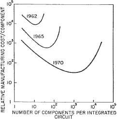
the cost per component. Thus there is a minimum cost
at any given time in the evolution of the technology. At
present, it is reached when 50 components are used per
circuit. But the minimum is rising rapidly while the entire
cost curve is falling (see graph). If we look ahead ve
years, a plot of costs suggests that the minimum cost per
component might be expected in circuits with about 1000
components per circuit (providing such circuit functions
can be produced in moderate quantities). In 1970, the
manufacturing cost per component can be expected to be
only a tenth of the present cost.
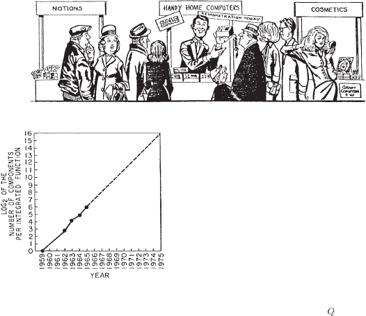
The complexity for minimum component costs has in-
creased at a rate of roughly a factor of two per year
(see graph). Certainly over the short term this rate can be
expected to continue, if not to increase. Over the longer
term, the rate of increase is a bit more uncertain, although
there is no reason to believe it will not remain nearly
constant for at least ten years. That means by 1975, the
number of components per integrated circuit for minimum
cost will be 65 000.
I believe that such a large circuit can be built on a single
wafer.
Fig. 1.
V. TWO-MIL SQUARES
With the dimensional tolerances already being employed
in integrated circuits, isolated high-performance transistors
can be built on centers two-thousandths of an inch apart.
Such a two-mil square can also contain several kilohms
of resistance or a few diodes. This allows at least 500
components per linear inch or a quarter million per square
inch. Thus, 65 000 components need occupy only about
one-fourth a square inch.
On the silicon wafer currently used, usually an inch or
more in diameter, there is ample room for such a structure if
the components can be closely packed with no space wasted
for interconnection patterns. This is realistic, since efforts to
achieve a level of complexity above the presently available
integrated circuits are already under way using multilayer
metallization patterns separated by dielectric lms. Such a
density of components can be achieved by present optical
techniques and does not require the more exotic techniques,
such as electron beam operations, which are being studied
to make even smaller structures.
VI. I
NCREASING THE YIELD
There is no fundamental obstacle to achieving device
yields of 100%. At present, packaging costs so far exceed
the cost of the semiconductor structure itself that there is no
incentive to improve yields, but they can be raised as high
as is economically justied. No barrier exists comparable
to the thermodynamic equilibrium considerations that often
limit yields in chemical reactions; it is not even necessary
to do any fundamental research or to replace present
processes. Only the engineering effort is needed.
In the early days of integrated circuitry, when yields were
extremely low, there was such incentive. Today ordinary
integrated circuits are made with yields comparable with
those obtained for individual semiconductor devices. The
same pattern will make larger arrays economical, if other
considerations make such arrays desirable.
MOORE: CRAMMING COMPONENTS ONTO INTEGRATED CIRCUITS 83
Copyright © National Academy of Sciences. All rights reserved.
The Future of Computing Performance: Game Over or Next Level?
172 THE FUTURE OF COMPUTING PERFORMANCE
Fig. 2.
Fig. 3.
VII. HEAT PROBLEM
Will it be possible to remove the heat generated by tens
of thousands of components in a single silicon chip?
If we could shrink the volume of a standard high-
speed digital computer to that required for the components
themselves, we would expect it to glow brightly with
present power dissipation. But it won’t happen with in-
tegrated circuits. Since integrated electronic structures are
two dimensional, they have a surface available for cooling
close to each center of heat generation. In addition, power is
needed primarily to drive the various lines and capacitances
associated with the system. As long as a function is conned
to a small area on a wafer, the amount of capacitance
which must be driven is distinctly limited. In fact, shrinking
dimensions on an integrated structure makes it possible to
operate the structure at higher speed for the same power
per unit area.
VIII. D
AY OF RECKONING
Clearly, we will be able to build such component-
crammed equipment. Next, we ask under what circum-
stances we should do it. The total cost of making a
particular system function must be minimized. To do so,
we could amortize the engineering over several identical
items, or evolve exible techniques for the engineering of
large functions so that no disproportionate expense need
be borne by a particular array. Perhaps newly devised
design automation procedures could translate from logic
diagram to technological realization without any special
engineering.
It may prove to be more economical to build large
systems out of smaller functions, which are separately pack-
aged and interconnected. The availability of large functions,
combined with functional design and construction, should
allow the manufacturer of large systems to design and
construct a considerable variety of equipment both rapidly
and economically.
IX. L
INEAR CIRCUITRY
Integration will not change linear systems as radically as
digital systems. Still, a considerable degree of integration
will be achieved with linear circuits. The lack of large-
value capacitors and inductors is the greatest fundamental
limitation to integrated electronics in the linear area.
By their very nature, such elements require the storage
of energy in a volume. For high
it is necessary that the
volume be large. The incompatibility of large volume and
integrated electronics is obvious from the terms themselves.
Certain resonance phenomena, such as those in piezoelec-
tric crystals, can be expected to have some applications for
tuning functions, but inductors and capacitors will be with
us for some time.
The integrated RF amplier of the future might well con-
sist of integrated stages of gain, giving high performance
at minimum cost, interspersed with relatively large tuning
elements.
Other linear functions will be changed considerably. The
matching and tracking of similar components in integrated
structures will allow the design of differential ampliers of
greatly improved performance. The use of thermal feedback
effects to stabilize integrated structures to a small fraction
of a degree will allow the construction of oscillators with
crystal stability.
Even in the microwave area, structures included in the
denition of integrated electronics will become increasingly
important. The ability to make and assemble components
small compared with the wavelengths involved will allow
the use of lumped parameter design, at least at the lower
frequencies. It is difcult to predict at the present time
just how extensive the invasion of the microwave area by
integrated electronics will be. The successful realization of
such items as phased-array antennas, for example, using a
multiplicity of integrated microwave power sources, could
completely revolutionize radar.
84 PROCEEDINGS OF THE IEEE, VOL. 86, NO. 1, JANUARY 1998
Copyright © National Academy of Sciences. All rights reserved.
The Future of Computing Performance: Game Over or Next Level?
APPENDIX C 173
G. E. Moore is one of the new breed of elec-
tronic engineers, schooled in the physical sci-
ences rather than in electronics. He earned a B.S.
degree in chemistry from the University of Cal-
ifornia and a Ph.D. degree in physical chemistry
from the California Institute of Technology. He
was one of the founders of Fairchild Semicon-
ductor and has been Director of the research and
development laboratories since 1959.
MOORE: CRAMMING COMPONENTS ONTO INTEGRATED CIRCUITS 85
Copyright © National Academy of Sciences. All rights reserved.
The Future of Computing Performance: Game Over or Next Level?
D
Reprint of Robert H. Dennard’s
“Design of Ion-Implanted MOSFET’s
with Very Small Physical Dimensions”
NOTE: Reprinted from Robert H. Dennard, Fritz H. Gaensslen, Hwa-Nien Yu, V. Leo
Rideout, Ernest Bassous, and Andre R. LeBlanc, 1974, Design of ion-implanted MOSFETS
with very small physical dimensions, IEEE Journal of Solid State Circuits 9(5):256 with per-
mission of IEEE and Robert H. Dennard © 1974 IEEE.
174
Copyright © National Academy of Sciences. All rights reserved.
The Future of Computing Performance: Game Over or Next Level?
APPENDIX D 175