Yellampalli S. (ed.) Carbon Nanotubes - Synthesis, Characterization, Applications
Подождите немного. Документ загружается.

3
Synthesis of Carbon Nanostructures
by Microwave Irradiation
J. Vivas-Castro
1
, G. Rueda-Morales
1
, G. Ortega-Cervantez
1
,
J. Ortiz-López
1
, L. Moreno-Ruiz
2
and M. Ortega-Avilés
2
1
Escuela Superior de Física y Matemáticas, Instituto Politécnico Nacional,
2
Centro de Nanociencias y Micro-Nanotecnologías, I.P.N.,
Mexico
1. Introduction
Carbon nanotubes (CNT) have been synthesized with various techniques of which the most
common ones are laser ablation, electric arc discharge, and chemical vapor deposition.
These methods produce CNTs with different characteristics, sometimes involving complex
experimental setups that add to their cost of production. It is of current general interest the
development of new techniques for the efficient and selective synthesis of CNTs and other
carbon nanostructures at the cheapest possible cost. One such possibility is the use of
microwave radiation, which over the past few years has played an important role as a
thermal tool in organic synthesis due to considerable advantages over conventional
methods (Lidström, et al., 2001). The use of microwave radiation in the synthesis and
functionalization of carbon nanotubes or other nanostructures is advantageous because it
provides a fast and uniform heating rate that can be selectively directed towards a targeted
area. The first report of the production of carbon nanostructures with microwaves was made
by Ikeda et al (Ikeda et al., 1995), who synthesized fullerenes from microwave-induced
naphthalene-nitrogen plasma at atmospheric pressure inside a cylindrical coaxial cavity. O.
Kharissova has reported the synthesis of vertically aligned carbon nanotubes using a
domestic microwave oven (Kharissova, 2004).
Graphite is a good microwave radiation absorber. It has been used in military applications
as radar-absorbing material and in anti-electromagnetic interference coatings for civil
purposes. Milled flake graphite and carbon nanotubes have microwave absorption maxima
in the 10-15 GHz frequency range (Fan et al., 2009). Microwave radiation can heat or cause
arcing in many objects and powdered samples can absorb such radiation and be heated
efficiently. Short-time direct exposure to microwave irradiation has been used to produce
exfoliated graphite as well as to reduce graphite oxide (Zhu et al., 2010).
In graphite powder, absorbed microwave radiation is converted into heat via dielectric loss
and conductive loss mechanisms. Graphite powder is oxidized by long exposure to ambient
air and may become partly electrically insulating. Microwaves are absorbed with energy
dissipation through the coupling of the radiation electric field with local electric dipoles
associated with structural defects in graphite powder particles such as particle edges,
dangling bonds, C-O bonds, impurities and others. The electric field of microwaves also
drives electric currents with efficient generation of heat due to the highly diffusive transport

Carbon Nanotubes - Synthesis, Characterization, Applications
48
of π electrons within small defective graphite particles loosely interconnected between each
other.
In this work, we present results on the synthesis of various carbon nanostructures under
different preparation conditions using a domestic microwave oven as energy source.
Starting material is a mixture of graphite powder with iron acetate which is then subjected
to microwave irradiation under different conditions. Heating of mixed powders under
microwave irradiation decomposes iron acetate leaving small Fe particles that act as
catalysts for the synthesis of carbon nanostructures. Various nanostructures are obtained
depending on the way the starting material is prepared and exposed to microwaves as well
as on the time of exposure. We make a detailed description of the synthesis results in
dependence of those parameters. With this technique, we have obtained blocks of dense
arrays of aligned multiwall carbon nanotubes, disordered nanotubes intercalated in between
graphite planes, long iron-filled multiwall carbon nanotubes, and other peculiar formations.
In addition, we propose mechanisms to explain how the synthesis of these nanostructures
takes place.
2. Experimental methods and materials
All the material obtained in this work was produced with the aid of a conventional domestic
microwave oven operating at 2.45 GHz (12 cm wavelength) with 1000 W power. Starting
material was prepared by mixing 30 wt% of iron (II) acetate (ferrous acetate, Fe(CO
2
CH
3
)
2
)
from Sigma-Aldrich (99.999% purity) with 70 wt% graphite powders (99.99% purity, particle
size less than 75 μm). The powders were then mixed and placed inside quartz ampoules (8
mm inner diameter, 10 cm long) which were then sealed under vacuum (10
−
4
torr).
Temperature of microwave-irradiated ampoules rapidly rises and stabilizes within an
elapsed time (few seconds) that depends on sample mass. The final temperature correlates
linearly with total mass. It has been reported that 0.25 g of graphite powder irradiated inside
a 700 W microwave oven reaches about 1000 °C in 12 seconds (Curling et al., 2009).
Microwave irradiation decomposes iron acetate into small Fe particles and at the same time
produces thermal swelling of graphite particles inside the ampoules. Various molecular
species resulting from thermal decomposition of the iron acetate molecule participate in the
chemical reduction of the oxide layer that forms on the surface of graphite and metallic
particles and make them catalytically active. Once formed, small Fe particles will also
absorb microwave radiation (Liu et al., 2006) and participate in further heating the powder
mixture. At initial stages of irradiation, metallic particles are small and eventually coalesce
into larger ones. At the same time, they will combine with graphite to form iron carbide
from which various nanostructures are generated. Evaporation of the catalytic metal will
occur in the case of direct exposure to microwaves because inside the ampoules the mixed
powders reach high enough temperatures. Evaporated iron will ultimately condense on the
ampoule walls and act as catalyst for the growth of dense arrays of aligned nanotubes.
Quite different products may be obtained by variations in the preparation conditions. We
have applied the following: (a) quartz ampoules containing the mixed powders may be
sealed under ambient air or under vacuum; (b) the ampoules can be partially submerged in
water inside the oven to avoid excessive heating and exposure to microwaves, and (c) direct
exposure of the ampoules to microwaves during short periods.
The resulting material was analyzed with scanning electron microscopy (SEM) using a FEI-
Sirion instrument operated at 5 kV with secondary electrons. Scanning-transmission

Synthesis of Carbon Nanostructuresby Microwave Irradiation
49
electron microscopy (STEM) was performed with a FEI Quanta Dual Beam instrument.
Transmission electron microscopy (TEM) was also employed for the analysis using a JEOL
200 C (200 kV) instrument as well as a FEI-Titan 80-300 with spherical aberration correction
(Cs TEM). For determination of the crystalline structure of metal particles inside MWNTs, a
double-tilt TEM sample holder was used. For examination with Raman scattering
spectroscopy we used two instruments: a Perkin-Elmer Raman Station 400F and a Horiba
Jobin Yvon LabRam HR800. For SEM and Raman studies, samples were analyzed ‘as grown’
with no special preparation. For TEM analysis, suspensions were prepared either in
dichloroethane or in deionized water with 0.5 wt% SDBS (dodecylbenzenesulfonic acid)
surfactant. To optimize dispersion of sample particles, the suspensions were sonicated in an
ultrasonic bath or using a 750 watt ultrasonic tip (Sonics) and later were centrifuged at
16,000 rpm. Samples for STEM and TEM analysis were taken from the supernatant material
and deposited by dripping in 300 mesh holey carbon TEM copper grids.
3. Description of synthesized material
3.1 Irradiation of quartz ampoules partially submerged in water
To retard sample reactions, we avoided direct microwave irradiation of the mixed powders
by partially submerging the prepared ampoules in water. In this way, most of microwave
radiation is absorbed by water and only a fraction of the radiation acts on the sample. The
consequence of this is that the material temperature rises more slowly and reactions in the
synthesis process will take longer to occur. We estimate that in our case, with our 1000 W
oven, the material reaches 1000 °C after 30 minutes. We prepared four samples (all of them
evacuated ampoules) with 30, 60, 90 and 120 minutes irradiation time at full power with the
turning plate of the oven in operation. Material produced under direct irradiation is
distinctly different and will be described separately.
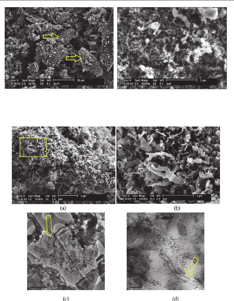
Carbon nanotubes (CNT) grow disorderly on the surface of graphite particles after 30 min
irradiation, as can be seen in the particle indicated with the lower arrow in Fig. 1(a). Fig. 1(b)
is a magnified view of the same particle where CNTs are clearly seen having curled
geometry and a wide distribution of diameters. Statistical analysis in the zone of the sample
corresponding to Fig 1(b) reveals that 3% of the tubes have diameters in the 4-10 nm range,
40% in the 10-20 nm range, 25% in the 20-30 nm range and the rest are wider than 30 nm. At
this stage, some graphite particles have not completely reacted with iron particles and
remain with flat surfaces, as shown with the upper arrow in Fig. 1(a).
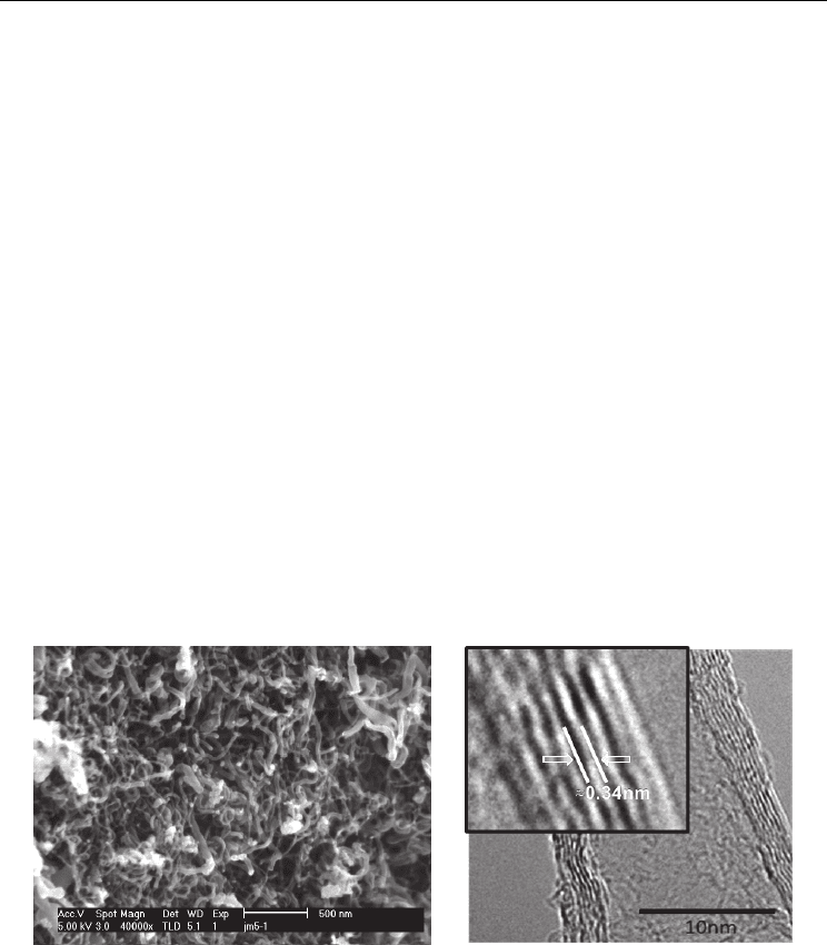
In samples with 60 min exposure (Fig. 2), CNTs are more abundant and other types of
structures appear. This is the case of Fig. 2(a) where a disordered arrangement of ‘worm-
like’ strips about 0.5 μm wide is observed. Fig. 2(b) shows a magnified view of the zone
marked with the rectangle in Fig. 2(a). The worm-like features seem to be formed by small-
area graphite layers that have slipped and displaced with respect to each other. Analysis of
this sample with transmission electron microscopy reveals the presence of graphite nano
particles, graphene layers, encapsulated iron particles inside multiwall carbon nanotubes
(MWNT) in different stages of growth, iron-filled graphitic onions and peapod-like
structures. Two examples of these structures are shown in Fig. 2(c) and (d). In Fig. 2(c) the
arrow marks a series of free graphene layers as a result of exfoliated graphite particles, and
Fig. 2(d) marks with an arrow a peapod-like structure inside a double-walled nanotube.
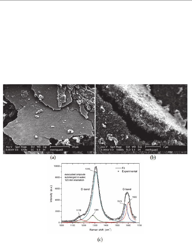
For the sample with 90 min exposure in Fig. 3, curled and disordered MWNTs dominate the
type of structures observed as seen in Fig. 3(a). TEM image in Fig. 3(b) demonstrates that
these nanotubes are indeed (defective) MWNTs, with irregular number of wavy walls
separated 0.34 nm.
Carbon Nanotubes - Synthesis, Characterization, Applications
50
(a) (b)
Fig. 1. SEM images of material obtained in an evacuated ampoule submerged in water after
30 min microwave irradiation: a) view at low magnification; b) view at higher magnification
of the surface of particle indicated by lower arrow in (a).
Fig. 2. SEM images of material obtained in an evacuated ampoule submerged in water after
60 min microwave irradiation: a) view at low magnification; b) higher magnification of the
rectangular zone marked in (a); c) TEM image of graphene layers marked with an arrow; d)
TEM image of a peapod-like structure marked with an arrow.
Synthesis of Carbon Nanostructuresby Microwave Irradiation
51
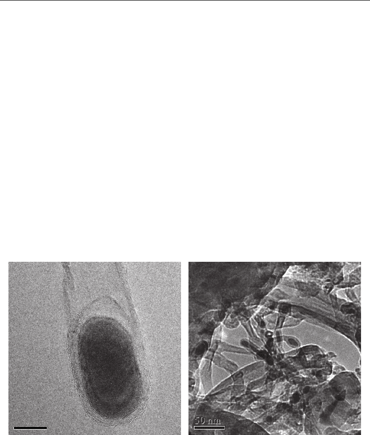
After 120 min irradiation, the majority of the original graphite powder has reacted with iron
catalytic particles and has been converted into MWNT. Large (more than 100 μm) and thin
(about 2 μm) blocks of disordered MWNTs can be collected on the ampoule walls as seen in
Fig. 4(a). The distribution of MWNT diameters falls in the 10-30 nm range. The magnified
image of Fig. 4(b) shows a cross sectional view of a fractured block revealing that the blocks
are highly porous and have the appearance of metal sponge.
Raman spectroscopy was performed for all samples prepared in evacuated ampoules
submerged in water. Their spectra do not display great differences with respect to the
irradiation time. Fig. 4(c) shows the Raman response (785 nm excitation, E
laser
=1.58 eV) of
the sample irradiated 120 min which illustrates the typical spectrum observed in other
samples. The signal is dominated by a large and wide D-band (1100-1400 cm
-1
) with a
shoulder around 1176 cm
-1
and a smaller G-band (1500-1700 cm
-1
). The spectrum has
features typical of nano graphite (Pimenta et al., 2007), but in view of our SEM and TEM
observations, the signal of a large amount of disordered and defective MWNTs should be
also present. A lorentzian line shape analysis reveals some possible component bands as
shown in Fig. 4(c). The measured G band has two components, the first one at 1578 cm
-1
,
associated with tangential modes in graphite or MWNT and the second one at 1602 cm
-1
, to
the D´ defect induced band in sp
2
carbons (graphite and MWNTs). The D band can be
decomposed in two main components at 1281 and 1310 cm
-1
as is usual in disordered
graphite and MWNTs (Dresselhaus et al., 2005). We identify the shoulder at 1176 cm
-1
as the
manifestation of a weak dispersive mode (sometimes called T-mode) observed in disordered
MWNTs, graphite, and other non-planar sp
2
carbons in the 1084-1100 cm
-1
range
(Kawashima, 1995; Li, 1997; Tan, 2004). As seen in our SEM and TEM images, all those types
of carbon structures may coexist in our highly inhomogeneous samples.
(a) (b)
Fig. 3. Material obtained in an evacuated ampoule submerged in water after 90 min
microwave irradiation: a) SEM image of a group of disordered nanotubes; b) TEM image
showing that the observed tubes are multiwall; the insert shows a magnified view indicating
a 0.34 nm interwall separation.
In samples obtained from ampoules submerged in water, small iron particles are attached to
the tips of the observed MWNTs, as shown in the TEM image of Fig. 5. For samples
prepared under direct irradiation, higher temperatures and stronger temperature gradients
induce complete filling of MWNTs interior with metallic iron as described in next section. In
Carbon Nanotubes - Synthesis, Characterization, Applications
52
Fig. 5(a) we observe an elongated iron particle (16 by 28 nm in size) attached to the end of a
MWNT and covered by several graphitic layers. Few new layers are seen forming inside the
tube as the MWNT grows behind the tip. For the same sample, Fig. 5(b) shows of a group of
MWNTs of various diameters, some of them as wide as 50 nm and others as thin as 10 nm,
the latter ones with an iron particle at their tip.
3.2 Direct irradiation of quartz ampoules
With direct irradiation, temperature of the mixed powders rises rapidly in few seconds.
Reactions are very fast and may become so violent that can cause explosion of the ampoules.
Care must be taken to avoid accidents for this reason. To perform these experiments we
previously determined the sites inside the microwave oven with maximum radiation
intensity. The ampoules (all of them evacuated) were placed horizontally, so that their
bottom (filled with the powder mixture) coincided with one of these sites.
Fig. 4. SEM images of material obtained in an evacuated ampoule submerged in water after
120 min microwave irradiation: a) large blocks of disordered nanotubes collected from the
ampoule walls; b) cross sectional view of a fractured block showing that it is entirely
composed of disordered MWNTs; (c) Typical Raman spectrum at 785 nm excitation of
material obtained after 120 min microwave exposure.
Synthesis of Carbon Nanostructuresby Microwave Irradiation
53
Fig. 6(a) illustrates SEM images of material collected from the ampoule inner walls after 10
min exposure to microwaves. The material is formed by blocks 7 to 10 μm thick of aligned
MWNTs also known as CNT ‘forests’ or ‘carpets’. Fig. 6(b), a magnified view of the zone
marked with the rectangle in Fig. 6(a), indicates a diameter distribution within the 40-60 nm
range. These CNT forests grow from iron particles produced by thermal decomposition of
the acetate that accumulate on the inner walls of the ampoules. In Fig. 6(c) we present a
Raman spectrum of the same sample. Defect D and tangential G bands are the strongest
features of the measured spectrum. The D-band is almost as large as the G-band indicative
of a sample with rather defective MWNTs and graphitic particles. At low energy there is a
weak feature around 319 cm
-1
whose nature is unclear but could be attributed either to iron
oxide, iron carbide or nano Fe crystals which become Raman active at small size. Another
weak and narrow feature can be found at about 1450 cm
-1
, in between D and G bands, which
is identified as an LO or defective mode (Dresselhaus, 2005; Gupta et al., 2006). Other weak
features in the Raman spectra of Fig. 6(c) include two small bands, one around 1750 cm
−1
(M-band) and the other around 1950 cm
−1
(iTOLA-band). The M-band consists of two
components, 1745 and 1788 cm
−1
, and it has been assigned to an overtone of the infrared-
active ‘out-of-plane’ mode (oTO) at 864 cm
−1
in sp
2
carbon materials (Brar et al., 2002). The
iTOLA-band at 1950 cm
−1
is identified as a combination of the in-plane transverse optic
(iTO) and longitudinal acoustic (LA) modes by the same authors. Other three notorious
features are identified as second harmonics and combination modes: (i) at 2427 cm
-1
, the G*-
band which is combination of defective D and T modes; (ii) at 2672 cm
-1
,
the G’-band which
is overtone of the D defective mode band, and (iii) at 2927 cm
-1
, the superposition of the
(a) (b)
Fig. 5. TEM images of material obtained in an evacuated ampoule submerged in water after
120 min microwave irradiation a) image of an iron particle at the tip of a MWNT; b) image
of a group of MWNTs of various diameters, the narrow ones with an iron particle at their
tip.
combined G+D modes and the overtone of the LO mode (Dresselhaus et al., 2005;
Kawashima, 1995; Shimada et al., 2005; Sveningsson et al., 2001; Tan, 2004). We note that the
2427 cm
-1
(G*) band has also been assigned to other combination modes (Maultzsch et al.,
10 n
m
10 n
m
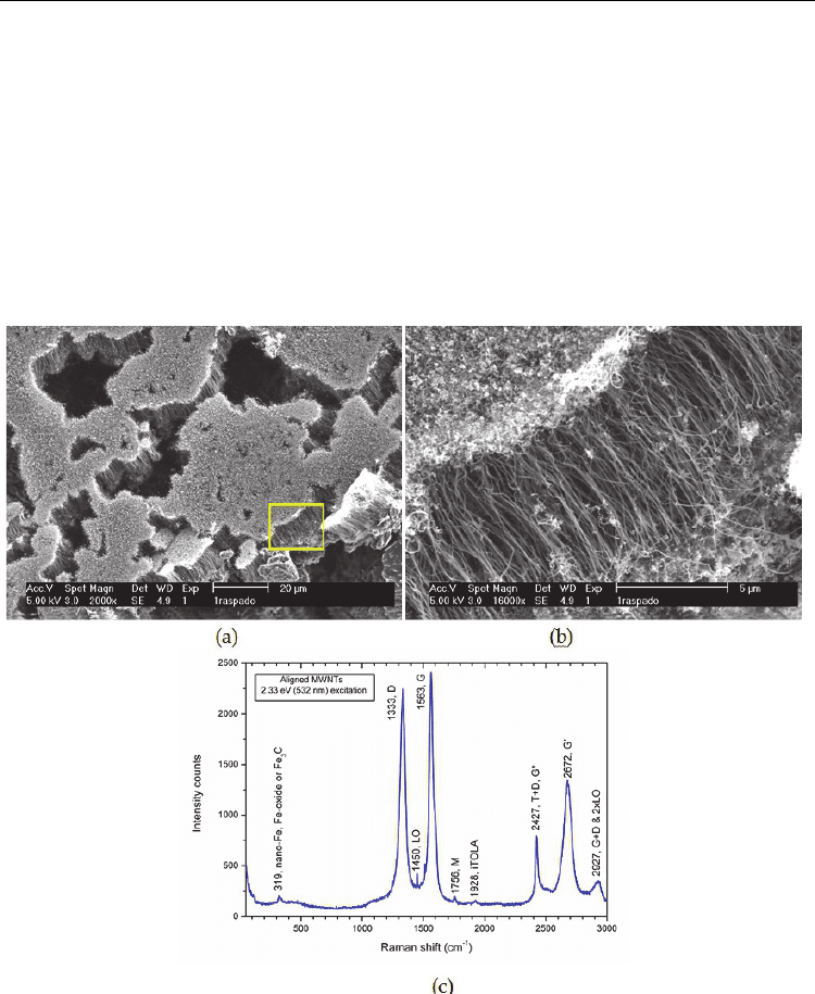
Carbon Nanotubes - Synthesis, Characterization, Applications
54
2004) and is usually a weak feature in most sp
2
carbons (Tan, 2004; Yoon, 2009) but in our
sample it is rather intense.
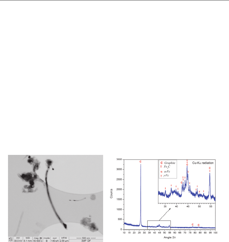
Another type of structure that can be obtained is iron-filled MWNTs as shown in the STEM
image of Fig. 7(a). The MWNT shown is of about 60 nm external diameter, while the iron
filling (in dark trace) is about 2 μm long and 15 nm diameter in its thinnest part. This result
was obtained with iron acetate catalyst and direct intermittent exposure to microwaves for
an effective time of 15 min. In Fig. 7(b) we present powder X-ray diffraction of the sample
corresponding to the image in Fig. 7(a). The identified reflections show the presence of
graphite particles (and MWNTs), α-Fe (cubic bcc) and γ-Fe (cubic fcc) crystalline iron as well
as iron carbide Fe
3
C (cementite), in agreement with nanostructured carbon material
synthesized with other techniques (Chen et al., 2004).
Fig. 6. Material obtained in an evacuated ampoule directly exposed to microwaves for 10
min: a) SEM image at low magnification of parallel arrays of aligned MWNTs; b) higher
magnification of the rectangular zone marked in (a); c) Raman spectrum at 532 nm excitation
of the same sample.
When the graphite/iron acetate powder mixture is finely ground and thoroughly mixed
with mortar and pestle, the time needed of microwave exposure for the synthesis of
Synthesis of Carbon Nanostructuresby Microwave Irradiation
55
nanostructures can be reduced substantially. Seven minutes of irradiation suffice for the
appearance of MWNTs and almost complete reaction of the powders. TEM analysis of a
sample prepared in this way shows abundant iron filled MWNTs as well as iron particles
attached to MWNT tips like the one shown in Fig. 8(a). We chose that particular MWNT for
structural identification of the metal particle at the tip using a double-tilt TEM sample
holder. The metal particle is relatively large (70 nm wide, 150 nm long) and, as we found
from its diffraction pattern, it consisted of several smaller ones of different composition and
structure. After few minutes of exposure to the electron beam, the large particle split into
smaller ones allowing determination of their individual diffraction patterns from spots close
to thin edges. Fig. 8(b) shows the situation after splitting of the original particle and tilting of
the sample holder to optimize crystalline orientation respect to the electron beam. Various
spots around particle edges were analyzed in detail. The specific spot marked with the
square in Fig. 8(b) is shown magnified in Fig. 8(c), in which crystalline planes of the metal
particle are clearly resolved. The area marked with the square in this image is further
magnified and shown in the inset at the upper left corner in Fig. 8(c). Below this magnified
view, its Fourier transform is also shown as inset in Fig. 8(c). The measured interplanar
distance is of 2.12 Å in the high resolution image of the inset, and the Fourier transform
identifies the crystalline structure as bcc oriented in [110] direction. From this we determine
that the particle corresponds to an α-Fe nanoparticle. From analysis of other spots we also
find γ-Fe nanoparticles (fcc structure) oriented in [111], as well as Fe
3
C nanoparticles
(orthorhombic structure). These results are in agreement with chemical analysis by energy
(a) (b)
Fig. 7. a) STEM image of iron-filled MWNTs from samples obtained by direct microwave
irradiation; b) X-ray diffraction pattern of sample corresponding to the image in a) in which
graphite C, α-Fe, γ-Fe and Fe
3
C phases are identified.
dispersive spectroscopy (EDS) which always showed presence of Fe and C and with the X-
ray diffraction pattern presented in Fig. 7(b).
4. Mechanisms of nanostructure formation
Both methods of irradiation described in this work result in somewhat different synthesized
material. Ampoules submerged in water are dynamically exposed to microwaves with
temperature gradients constantly changing because the ampoules themselves are set in

Carbon Nanotubes - Synthesis, Characterization, Applications
56
random rocking motion due to the surrounding boiling water. The resulting material in this
case are curled MWNTs for long exposure times. In the case of direct irradiation, exposure
to microwaves and temperature gradients are static, resulting in the growth of well oriented
and aligned MWNTs arrays. In spite of these contrasts, it is possible to elaborate models of
the mechanisms involved in the formation of the observed nanostructures.
For initial stages, when temperature is not too high, microwave absorption by graphite
particles thermally expands its layers, facilitating the intercalation of foreign species
between them (red particles), whilst exfoliation of outermost layers is also taking place. This
is described schematically in Fig. 9(a). At the same time, ferrous acetate in our mixed
powders is pyrolyzed above 200 °C
1
. Similar as reported for nickel acetate (Afsal et al.,
1991), pyrolysis of ferrous acetate proceeds according to the following reactions:
Fe(CO
2
CH
3
)
2
→ FeO + CH
3
COCH
3
+ CO
2
(1)
2 Fe(CO
2
CH
3
)
2
→ 2 FeO + 2 CH
3
COCH
3
+ 2 CO + O
2
(2)
In both reactions, thermal decomposition yields FeO (wustite), and volatile and gaseous
components such as acetone CH
3
COCH
3
, carbon monoxide, carbon dioxide and oxygen.
Acetone itself can reduce FeO into metallic Fe which will eventually combine with graphite
to form iron carbide Fe
3
C (cementite) from which carbon nanotubes and other
nanostructures grow. A possible route for this to happen is the following:
4 FeO + CH
3
COCH
3
→ Fe + Fe
3
C + 2 CO + 3 H
2
O (3)
Graphite particles in our powder mixture will provide feedstock for the growth of the
observed nanostructures either from reaction with metallic Fe or from the carbide Fe
3
C
obtained from the above reaction. At temperatures above 590 °C, acetone from reactions (1)
and (2) may decompose into methane CH
4
,
ethylene C
2
H
2
, carbon monoxide and ketene
CH
2
CO, as reported as early as 1929 (Rice et al., 1929). Methane and ketene may also act as
reduction agents of FeO. In relation to pyrolysis of acetone and methane, we should draw
attention to the early work of E. L. Evans and collaborators (Evans et al., 1973) who reported
the growth of filamentary carbonaceous deposits in the presence of iron, nickel and stainless
steel surfaces. In the case of acetone pyrolysis on iron surfaces, these authors found the
formation of lamellar γ-Fe
2
O
3
at temperatures as low as 400 °C. This last observation
indicates that pyrolysis and redox reactions of all chemical species involved may be quite
more complex than those implied by the simple reactions (1) - (3).
Metallic particles will interact differently with neighboring graphite grains depending on
their relative position respect to the graphite planes (graphene layers). It is expected that
catalytic reactivity will be facilitated when the metallic particle sits close to the edges of
graphite planes because it will readily interact with carbon end atoms. Evidence of this is
seen in the SEM image of Fig. 9(b) where a graphite grain has reacted with iron particles
mostly along its flanks (right arrow), while the uppermost layers look unaffected (left
arrow). When this occurs, carbon and metallic iron will combine into metallic carbide and a
carbon nanostructure will grow from the carbide particle as it becomes saturated with
carbon atoms. This growth mechanism for carbon nanotubes is well known in the literature
(Saito, 1995). If the metallic particles are small enough (less than 0.7 nm), they will react only
1
Sigma-Aldrich, material safety data sheet of iron (II) acetate
