Yellampalli S. (ed.) Carbon Nanotubes - Synthesis, Characterization, Applications
Подождите немного. Документ загружается.

Design and Demonstration of Carbon Nanotubes (CNTs)-Based Field Emission Device
427
a
b
c
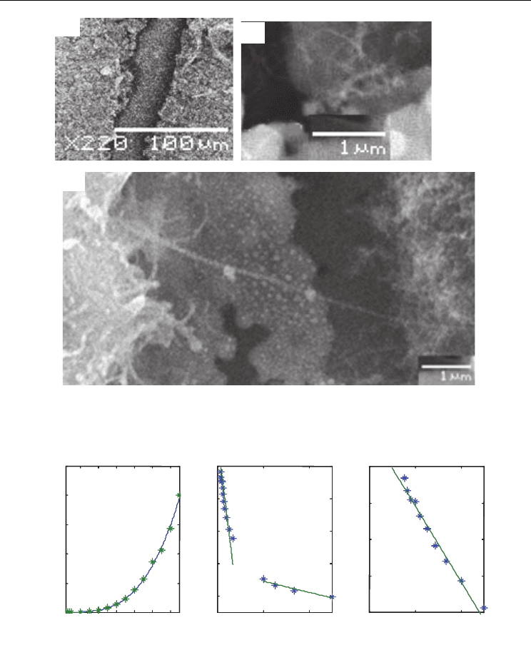
Fig. 1. (a) a trench etched with laser; (b) carbon nanotube on the edge of trench; (c) a carbon
nanotube with the length of 5µm
20
40 60 80 100120
0
0.5
1
1.5
2
2.5
x 10
-7
0 0.1
0.2
-29
-28
-27
-26
-25
0 0.01 0.02
-27
-26.5
-26
-25.5
-25
currents I/A
Ln
(
I/V
2
)
/ln
(
AV
-2
)
Ln
(
I/V
2
)
/ln
(
AV
-2
)
(a) Potential on electrode /V
(b) 1/v /V-1
(
c
)
1/v /
V
-1
a
b
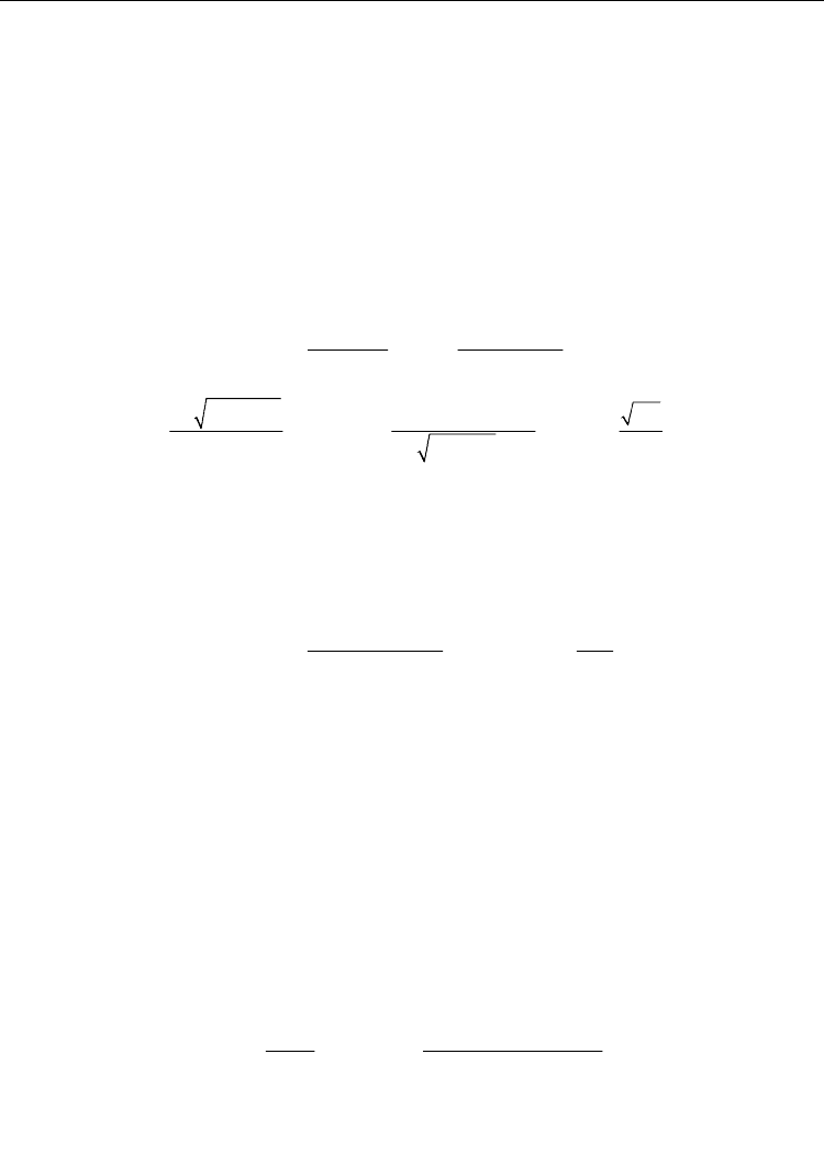
Fig. 2. (a). Emitting current vs. Voltage, (b). F-N plot(Potential ranged from 4V~130V)(c).
F-N plot(Potential ranged from 40V~130V)
insulation between the cathode and gate (the resistance between the cathode and gate
shoud be more than 50MΩ at least), but also ensuring CNTs left at the edge of the trench.
Then the field emission character of CNTs on both side of trench can be measured in
vacuums with a low current testing instrument (such as Cathely 6517A). Fig.1(a) shows

Carbon Nanotubes - Synthesis, Characterization, Applications
428
that a trench is etched on the silver layer mixed with CNTs by laser beam, in the middle of
which there are some little silver particles left, whose width is about 35um. There are
some CNTs on both side of the trench, rarely seen them in the middle of trench, which is
likely to be sputtered out with the silver particles. In the trench some longer CNTs can be
observed occasionally. Seeing Fig. 1(c), the length of a CNTs outside of the silver layer in
trench is about 5um. The edge of the trench is not very even and the length of CNTs is not
the same.
The character of CNTs field emission is shown as Fig. 2, which shows that the curve of
CNTs field emission matches very well with F-N curve when applied voltage between the
electrodes exceeds 40V ; while flaten a lot, when less than 40V. (shown as curve b in Fig. 2
(b)).
2.3 Theoretical prototype and analysis
In field emission experiments, the measured F-N curve is not a strict straight line which has
a little difference compared with the result deduced from the F-N Theory. As curve b in Fig.
2(b), this is a relatively common phenomenon, but people trend to show the emission
characteristic curve in specific voltage range, such as a curve in Fig. 2c. We have seldom
seen somebody explain the phenomenon shown as in curve a) and b) in Fig. 2b. From the F-
N formula,
22 73/2
6
( ) ( ) 6.83 10
(1.54 10 ) exp( )
()
iL LV
ALV
(1)
In equation (1), L is the length of CNTs and A is the effective emitting area of CNTs. It can be
observed that only two parameters that infulence the F-N curve slope, namely, the field
enhancement factor β and work function φ. For CNTs, β has something with the length,
radii, and the shape of the CNTs, while φ relates with the CNTs adsorption. In order to
explain the reason why the F-N curve slope in experiment changed with the voltage
changing, let us to suppose that the length distribution of CNTs at the edge of the trench
obeying with normal distribution, and CNTs shape at the up end and their radii are the
same, and each CNT field emission is independent of different field enhancement factor
β(L). So the total field emission current I is:
()()
l
IGLiL
(2)
In equation (2), G (L) is the number of the CNTs with the length distributed in the range of
L± 0.2µm, if some of the CNTs is shortend at the higher emission current because of heat or
bormbardment of the charged particles(in fact, the disappearance of some kind protroding
parts on the top of CNTs can be considered in the same way as that of shortening the length
of CNTs), so at different voltage, the length of CNTs have different cutoff values, which
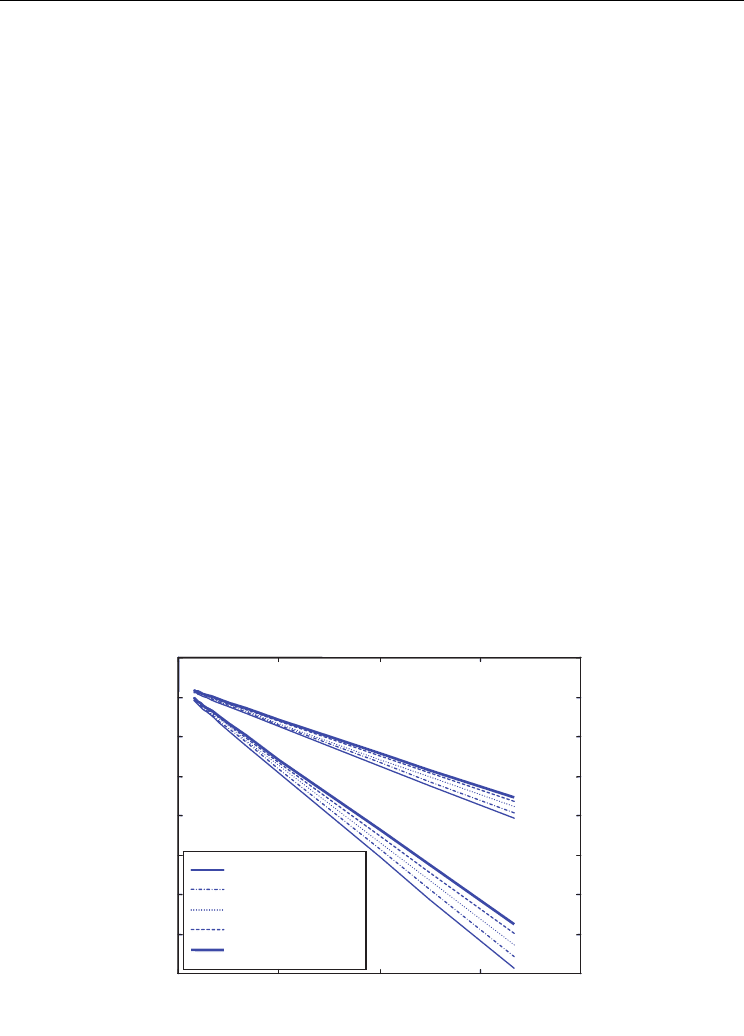
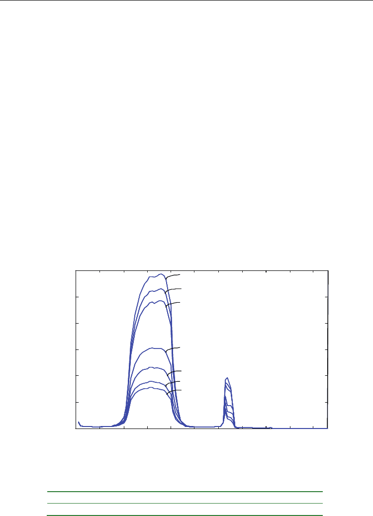
impact the CNTs field enhancement factor. Fig. 3 show the F-N curves at two different work
function and five different cutoff lengths. It can be seen that the shorter cutoff length is, the
greater the work function is, and the greater the slope of curves is. To be simple, we
supposed that the expected value of the CNTs length is 3µm, whose mean square deviation
is 1µm, and all the radii of CNTs is about 3nm.There are several methods about the
calculation of the field enhancement factor, for different length ranges[6,7]. We make use of
the calculation method β
(L)=KL/r commonly used for CNTs. Here K is the statistic of the
Design and Demonstration of Carbon Nanotubes (CNTs)-Based Field Emission Device
429
previous field enhancement factor and a correctable coefficient given when we choose CNTs
length ranges. Now the experimental phenomena can be explained below: At the low
voltage, the emission current is mainly emitted from longer CNTs, but little from shorter
ones. The longer the CNTs are, the greater the field enhancement factor is, and the smaller
the slope of F-N curve is. During this stage, the field emission process is dominated by the
CNTs in absorbate formed by water vapor, which can be formed into the C-H-O-H bond on
the surface of CNTs, and reduces the effective work function of the CNTs surface
[8]
. These
two factors result in a smaller F-N curve slope ( φ
1.5
/β) at the beginning of the CNTs field
emission.
As the electric field intensity increases further, the CNTs field emission current increases
and the tiny protuberances on the tip of CNTs are melted or smoothened under
bombardment by residual gas particles. Meanwhile, the absorbate on the top of CNTs is also
removed, and then the effective work function increase to 5 eV, which is equal to that of net
carbon. It can be seen that the shorter CNTs and the greater work function will lead to the
greater slope of F-N curve, and the contribution of shorter CNTs to field emission is
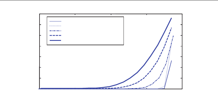
growing with the increasing of electric strength on the top of CNT. Fig. 4 show the values of
CNTs field emission current at different voltage and different cut-off lengths ranged from
1µm to 4.7µm, to a certain cut-off length, the lengths of CNTs follows the Guassian
distribution. It can be seen that: When the applied voltage is lower
(such as 6V), the
emission current is mainly contributed by CNTs of length 4.6µm or more; When the applied
voltage increases to 130V, the current emitted by CNTs with length of 2.8µm or more will
contribute a large proportion to the total. So we can get a conclusion: with the reduction of
CNTs length and increasing of its work function according to improvement of the voltage,
the slope of the F-N curve becomes more flat, When the applied voltage is more than 40V,
the field emission is mainly adopted by clean CNTs with work function of about 5eV, and
the F-N curve strictly follows a straight line ( shown as Fig. 2(c))
0 0.05 0.1 0.15 0.2
-160
-140
-120
-100
-80
-60
-40
-20
0
4.1
μ
m cutoff
4.3
μ
m cutoff
4.5μm cutoff
4.7
μ
m cutoff
4.9μm cutoff
Φ=3eV
Φ=5eV
Ln(I
c
/V
2
)/ln(AV
-2
)
1/v / v
-1
Fig. 3. F-N curves of different cutoff length and work function
Carbon Nanotubes - Synthesis, Characterization, Applications
430
1 2 3 4 5
0
1
2
3
4
5
6
7
x 10
-8
6V ×
(
3×10
51
)
40V ×
(
2×10
6
)
80V ×
(
70)
130V
10V ×
(
4×10
30
)
Len
g
th of carbon nanotube /
μ
m
Emit
t
ed current /A
Fig. 4. illustrating the varying contribution of tube length to total current I, for different
anode potentials V.
2.4 Conclusion
There are lots of field emission experiments about CNTs, but in many cases they just show
some field emission characters in specific voltage ranges, thus the result of experiments
matching well with F-N curves. Although some experiments get the CNTs field emission
character both at low and high electric field intensity, there are no reasonable explanation
about them. Based on the F-N tunneling theory, a simple prototype has been established in
the paper, which explains well the phenomenon that the slope of F-N curve changes with
applied electric field intensity in the process of CNTs field emission. The main reason for
increasing of F-N curve slope is considered that the adsorbate plays a big role at the
beginning of field emission, and then the field emission of carbon atoms on the surface of
CNTs becomes dominated gradually. Meanwhile, as the voltage increasing, the
protuberance on the top of CNTs disappears by bombardment of the remained gas particles.
In fact, the CNTs field emission is much more complex. First of all, the CNTs itself can be
classified into metallic and semiconductor according to the chirality. Secondly, the type of
materials adsorbed on the surface and their locations on top of the CNTs are all changed,
and the emission area is also a transformable factor. Consequently there will be lots of
theoretical and experimental work needed to be carried out if we want to have a more
intensive understanding about the process of CNTs field emission.
3. The Influence of relative height between cathode and gate on electron
transmission efficiency
3.1 The key points and technical background
This topic associates with the structure optimization design for a kind field emission display
(FED), among the parameters affecting FED performance, the relative height between
cathode and gate plays an important role because it dominates FED electron transmission
efficiency directly. The electron trajectories as well as their distribution on anode in a large
area-full colored FED prototype have been theoretically analyzed by using Monte Carlo and
Boundary Element Methods. The result has been used to improve the electron transmission
Design and Demonstration of Carbon Nanotubes (CNTs)-Based Field Emission Device
431
efficiency via adjusting the vertical distance between cathode and gate, at the same time, the
elevation angle of CNT on the influence of transmission efficiency is also discussed.
It is noted that the surface conduction electron emitter displays
[1]
(SCED) proposed by Canon
Corporation has simplified production process of FED, and provided a feasible way for FED
with large area. According to the technical information, the electron transmission
efficiency(the ratio of electron to the anode and electron to the cathode) of this kind is no
more than 1%, so we proposed two solutions to try to improve it
[9]
: First, using CNTs
instead of P
d
O emitter, thus the electron transmission efficiency can be adjusted by
controlling the direction of CNTs , theoretical calculations prove that when the angle
between CNTs and gate plane reach 30°, almost all electrons can reach the anode and form
the emission current; Meanwhile, giving the symmetrical axis of CNT parallel to the gate
plane, we can also improve the electron transmission efficiency according to enlarging the
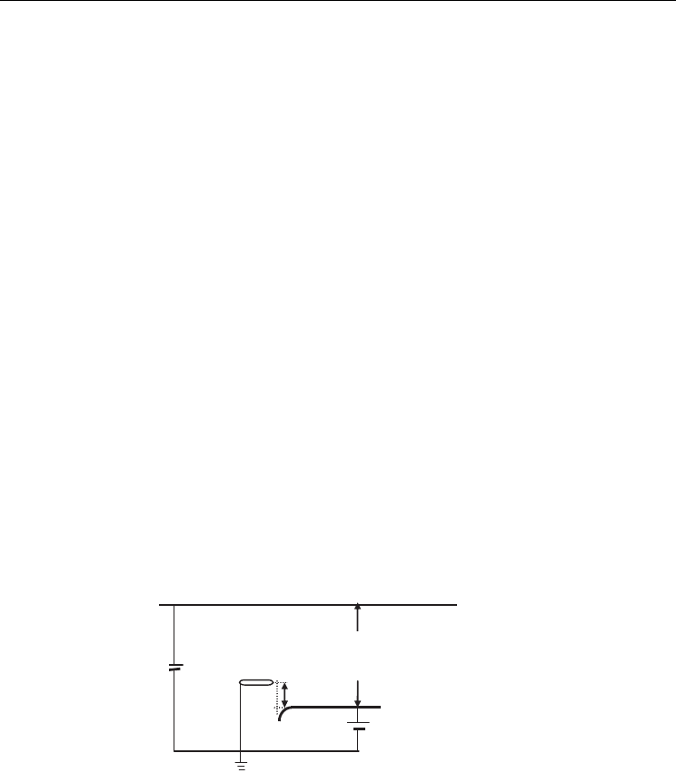
relative height between gate and cathode(as shown in Fig. 5).
3.2 The structural and theoretical model of the FED’s
Fig.5 is a simplified structural model of one FED pixel, in which the emission cathode
consists of CNTs, whose symmetrical axis are parallel to the gate and anode planes,
supposing the CNT is 2µm long, and closed by a hemisphere with radius 2.5nm on the top.
The distance between anode and gate is 1.5 mm. The side of gate near the CNTs is a quarter
arc with radius 0.05µm. By chiral vector, CNTs can be divided into metal and
semiconductors which have different band gap. Giving the chiral vectors are uniform
distributed, there would be one third of the metal and two thirds of the semiconductor in all
type of the carbon tubes
[10]
. But the experimental results of O.Groning
[7]
indicate that CNT’s
field emission characters fit the theoretical model of metal field emission. The experiments
of J.M.Bonard
[11]
demonstrate that, in the case of small current, field emission characters of
CNTs fit Fowler-Nordheim formula. So we simplified the CNTs as a metallic cylindrical
shell with the end closed by a hemisphere.
O
Va
Vg
cathode
anode
gate
1.5m
m
P
Δ
Fig. 5. Model of electric structure
Both the dimension of the electrodes and the distance between them are particularly
different (the distance between anode and cathode is 300,000 times than the diameter of
CNTs)
which brings about the electric field distribution is extremely uneven in the border
region, so that the Boundary Element Method (BEM) is an ideal one to calculate the electric
distribution on the domain of our interest
[12]
. 106 units are divided on all the electrodes
consisting the boundary of one sub-pixel: cathode( CNT), gate and anode. Considering the
quite imbalance of charge density distribution in each electrode, especially the charge
Carbon Nanotubes - Synthesis, Characterization, Applications
432
density in the cathode is much higher than what in the anode. So that the length of each unit
is different in the process of dividing the border, boundary elements tend to put a greater
element density where they are needed, such as near the end of electrodes and in regions of
high curvature. There are 62 units on the CNTs, 20 units on the gate, and 24 units on the
anode. The distribution of initial position, velocity, elevation and intensity of electrons
launched by CNT is sampled with Monte Carlo Method.
(1). Localization the initial position of electrons
For an electron launched by emitter, how to decide which discrete unit it is from? For given
temperature T and work function E
Ф
, the higher the field intensity, the more probability of
electrons can be emitted. According to Fowler-Nordheim formula, the current density
emitted from the cathode can be expressed below
[13] [14]
:
3
4/
() exp( )
sin( / )
emkTd kT d
JT c
hkTd
(3)
In equation (3),
3
0
82||
()
3
mE
cv
y
he
0
42||()
he
d
mE ty
3
0
e
y
E
Where
e is electron charge, m is electron mass, k is Boltzman constant, h is Planck constant, ε
is electric field strength,
φ
E is work function of emitter,
0
()ty is close to 1,
0
()y
is the
Nordheim Function,
T is the temperature of cathode, When equation (3) is normalized, it
can be used as emission probability function for cold field emission, so the normalized
emission probability density function
1
()f
can be expressed as:
3/2
62
7
1 0
23
1.54 10
( ) (0) / exp[ 6.83 10 ( )]
(/)
M
M
E
f
JJ vy
JEt e E
(4)
In equation (4),
Ј
M
is normalized constant. Using expression (4), we can sample the electric
density
ε with Rejection Selection Method
[15]
. In principle, ε can be any value in [0, ∞], in
order to improve sampling efficiency, we just sample in [
1.0, ε
m
]×10
7
V/cm. because for cold
cathode, the obvious electron emission occurred only when the electric field intensity of
emitter surface is up to 2~3×10
7
V/cm, while ε
m
is the max electric field intensity on CNT’s.
After sampling a electric field intensity
ε, a comparison of sampling value is made with all
the electric field intensities on the nodes, among which the nearest field intensity of the
point is, the node is taken as the emitting position, which serve as the initial position of the
traced electrons, furthermore, the electric field intensity of these points can be used to
calculate the initial acceleration of electrons.
(2) Sampling the initial energies of emitted electrons
The number of electrons with initial energy in
E~E+dE is:
3
4exp[()/]
() exp( )
exp[( ) / ] 1
F
F
me E E d
I E dE d c dE
hEEkT
(5)
In equation (5),
E is the energy of emitted electron, E
F
is the Fermi energy, I(E) is the current
density with electron energy of
E, I
M
normalized constant, from equation (5), we can get
probability density function
2
()
f
E of initial energy below:

Design and Demonstration of Carbon Nanotubes (CNTs)-Based Field Emission Device
433
2
3
() 4 exp[( )/]
() exp( )
exp[( )/ ] 1
F
MM F
IE me E E d
fE d c
IIh EEkT
(6)
According to expression (6), we can sample initial energy of electrons with Rejection
Selection Method too. Because the energy spectrum of field emission electrons is very
narrow
[16]
, the electron energy is in the range of 1.5eV (even just 0.5eV
[18]
) around Fermi
level
[16] [17]
, M. J. Fransen, et al
[18]
have measured the FWHM of CNTs field emission is
0.11~0.70eV, so we will sample of the emission electrons in 4.8~5.3eV for improving the
sampling efficiency.
(3) Elevation angle
α of emitted electrons in each unit obeys Lambert’s Law, that is:
3
2cos 0 cos 1
(cos )
0
f
else
(7)
From expression (7), we can sample the elevation angle α of emitted electron.
Assuming T=300K in the cathode emitter, the CNT’s work function
[11] [15] [16]
E
=5.0eV,
0
()1ty . When we completed the sampling of initial position, initial energy and emission
direction according with the above steps, the initial state (position, elevation angle,
acceleration and velocity) of electrons were completely determined. Then tracing the
trajectories of electrons, among them the electrons reached the gate are called the
conduction electrons, and those reached the anode called the emission electrons, which
eventually bombard the screen to form image information.
3.3 The results and analysis
In the calculation process, let anode voltage Va=4000V, gate voltage Vg=50V. Fig.6 expresses
the electric field intensities of every node on the boundary when the distance Δ of CNT’s
axes above the gate is changed. It is clear that the electric field intensities of CNT’s tip can
reach strength for field emission; furthermore, the electric field intensity of CNT’s tip is
three orders of magnitude higher than the electric field intensity on anode. When Δ=0, the
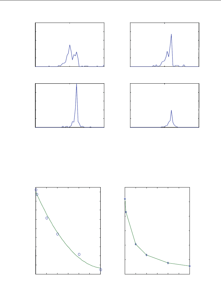
minimum distance between CNT’s apex and gate is 20.7nm. Fig.7 a, b, c and d show that the
distributions of electrons reaching the anode with Δ=300nm, 50nm, 5nm, and 0(assuming in
each case, the number of electrons is identical) respectively, while the area under the curve
represents the number of electrons reaching the anode. With the increasing of Δ, the electron
beam has a tendency of dividing into two beams. But on the whole, focusing of electron
beam is rather ideal, the smaller Δ is, the better it focused. When Δ=5nm, the FWHM of
electron beam spot is less than 50μm. With Δ changing, the center of the electron beam
remains always at about 100μm at the right side of the CNT. This phenomenon must be
taken into consideration in the process of the device package.
The relationship of electron transmission efficiency with the vertical distance Δ is shown in
table 1, when Δ decreasing from 300nm to 0, the electron transmission efficiency dropped
from 50.5% down to 17%. Therefore, the larger
Δ is, the less constrain the gate would act to
the electrons, which means the more electrons can break the restrain of the gate to reach the
anode and form the emission current. Fig.8a shows the changes of the actual total number of
electrons (logarithm) emitted at the top of CNT with
Δ changing. It can be seen that , for
both
Δ=300nm and Δ=0, the total number of electrons emitted from CNTs is 17 orders of
magnitude difference, that is to say, if there are two identical CNTs with
Δ=300nm and Δ=0,
Carbon Nanotubes - Synthesis, Characterization, Applications
434
the field emission of the CNT which is close to the gate will play a decisive role. Fig.8b
shows the change of the maximal strength of electric field on CNT’s tip with
Δ changing; No
doubt it will directly affect the current density of emission electrons. In fact, in its changing
process, the distance between CNT’s tip and gate is changing too, so it is difficult to
distinguish the main factors whether the vertical distance
Δ or the transactional distance
between CNT’s tip and gate that affect the electronic transmission efficiency is. So we can let
CNT in two specific position for comparison : in Fig.8, if the arc apex
O on the left of gates is
the origin of coordinates, so at two different emitting points P
1
(0, 100nm) and P
2
(-50nm,
50nm), in both positions, the distances between the emitting points and gate are all 61.8nm.,
but the electron transmission efficiency are 44.25% and 40.75% respectively, and it proves
that one can improve the electronic transmission efficiency by increasing
Δ, compared with
the experimental results of Canon corporation
[15]
, we can conclude that even if the CNTs
and the gate are in the same plane, the electron transmission efficiency can also be increased
only by increasing the transversal distance between cathode and gate, but it needs to
increase the voltage of the gate at the same time. In order to test the influence of CNT’s
angle on the electron transmission efficiency, we set the apex of CNT at coordinate (-
267.6nm, 1051.25nm) to calculate the transmission efficiencies when the elevation angles
equal to 30
°
and 0
°
, as a result, the corresponding electron transmission efficiency are 99.7%
and 64.7% respectively. It shows that the impact of electron emission direction on electronic
transmission efficiency is much greater, because the emission electrons have relative high
inertia, so there are more electrons can break the strong confinement of the gate and
eventually reach the anode.
0 10 20 30 40
5
0 60 70 80 90 100
0
1000
2000
3000
4000
5000
6000
node
Electric intensity on nodes (V/μm)
Va=4000V
Vg=50V
Δ
=200nm
Δ
=300nm
Δ
=100nm
Δ
=50nm
Δ
=10nm
Δ
=5nm
Δ
=0
Fig. 6. Relationship of electric intensity on nodes with vertical distance between cathode and
gate (the first 62 nodes on tube, the next 20 ones on gate and the last 24 ones on anode)
Δ(nm) 300 200 50 5 0
Efficiency η (%) 50.5 45.3 44.25 30.25 17
Table 1. Relationship of electron transmission efficiency with Δ
Design and Demonstration of Carbon Nanotubes (CNTs)-Based Field Emission Device
435
-500 0
500
0
0.2
0.4
0.6
0.8
1
-500 0
500
0
0.2
0.4
0.6
0.8
1
-500 0
500
0
0.2
0.4
0.6
0.8
1
-500 0
500
0
0.2
0.4
0.6
0.8
1
Δ
=300nm
Δ
=50nm
Δ
=5nm
Δ
=0
a b
c d
a.u a.u
a.u a.u
μ m
μ m
μ m
μ m
Electron intensity
Electron intensity
Electron intensity
Electron intensity
Fig. 7. Distribution of emitted electrons on anode (Va=4000V, Vg=50V, X axis representing
the X coordinate of emitted electrons, ranged from -500 to 500μm)
0 50 100 150 200 250
300
-12
-10
-8
-6
-4
-2
0
2
4
6
(a ) Vertical distance from cathode to gate /nm
Total emitted electrons/ l g.
0 50 100 150 200 250
300
1
2
3
4
5
6
7
(b) Vertical distance from cathode to gate/nm
Maximum electric intensity(V/m)
×10
7
Va=4000V
Vg=50V
Va=4000V
Vg=50V
Fig. 8. (a) Relationship of total emitted electrons with the vertical distance Δ (b) Relationship
of maximum electric intensity on cathode with Δ
Carbon Nanotubes - Synthesis, Characterization, Applications
436
3.4 Conclusion
Although the driving voltage of the FED with surface conduction of the Canon corporation
is lower (12V), but the distance between cathode and gate is just about 10nm, resulting in
the lower electron transmission efficiency, thus limiting the brightness of the display. By
increasing the distance between the cathode and gate and the relative height between
cathode and gate, especially increasing the elevation angle of CNTs, one can substantially
improve the electron transmission efficiency. On the other hand, the focusing performance
of electrons reaching anode would be worse, and the gate voltage has to increase, so that we
must make an appropriate choice among electron transmission efficiency, driving voltage,
resolution and simple arts and crafts.
4. Design and experiment on a field emission display prototype based on
CNTs
4.1 The main points and technical background
Display devices based on carbon materials are considered to be the best choice for field
emission large area displays (40” diagonal or larger). CNTs are capable of emitting high
currents (up to 1 A /cm
2
) at low fields (~5V/µm)
[16]
, and are believed to be ideal candidates
for the next generation of field emission flat panel displays and lighting elements. Choi
[17]
et
al
have demonstrated a fully sealed 4.5 in diode field-emission display using single-wall
CNT organic binder. In order to use CNTs as the electron field emitters for large-area
displays, it is desirable that an inexpensive substrate such as a lime glass plate can be used
for CNTs deposition. A patterned conductive layer needs to be formed on a glass plate
before CNT is coated onto the substrate and used as electrode lines. Because of the low
melting point of glass and the large mismatch in the coefficient of thermal expansion
between metal and glass, carbon deposition cannot be performed at too high a temperature.
Previous efforts have been concentrated on controlling the growth process to produce arrays
of aligned CNT on patterned substrates and have been successful in some aspects
[18~21]
. At
the same time, various low temperature chemical vapor deposition (CVD) techniques are
being studied to achieve low threshold field emission of electrons at a high emission current
density
[22][23]
. Vertically aligned CNTs have been synthesized by plasma- enhanced CVD
[1]
.
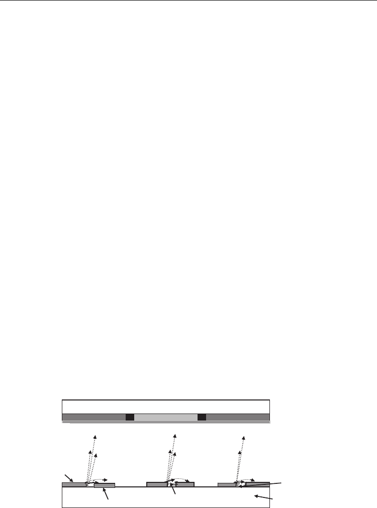
Fig. 9. Schematic structure of a pixel of the plat panel display
cathode
Gate
Front
g
lass
p
late
e
e
e
Ie
Ic
e
Patterned
p
hos
p
ho
r
Glass
p
late
e
e
Carbon nanotubes
Trench
Al film
Red
Green
Blue