Yellampalli S. (ed.) Carbon Nanotubes - Synthesis, Characterization, Applications
Подождите немного. Документ загружается.


Selective Growth of Carbon Nanotubes, and Their Applications
to Transparent Conductive Plastic Sheets and Optical Filters
97
Hecht D.S., Thomas D., Hu L., Ladous C., Lam T., Park Y., Irvin G., & Drzaic P. (2009).
Carbon-nanotube film on plastic as transparent electrode for resistive touch
screens. Journal of the Society for Information Display, Vol. 17, No. 11, (November
2009), pp. 941-946, ISSN 10710922
Hiramatsu M., Nagao H., Taniguchi M., Amano H., Ando Y., & Hori M. (2005).
High-Rate Growth of Films of Dense, Aligned Double-Walled
Carbon Nanotubes Using Microwave Plasma-Enhanced Chemical Vapor
Deposition. Japanese Journal Applied Physics, Vol. 44, No. 22, (May 2005), pp. L
693–L 695
Murakami Y., Chiashi S., Miyauchi Y., Hu M., Ogura M., Okubo T., & Maruyama S. (2004).
Growth of Vertically Aligned Single-Walled Carbon Nanotube Films on Quartz
Substrates and Their Optical Anisotropy. Chemical Physics Letters, Vol. 385, No. 3-4
(February 2004), pp. 298-303
Muramatsu H., Hayashi T., Kim Y. A., Endo M., Terrones M., & Dresselhaus M. S. (2005).
Growth of Double-Walled Carbon Nanotubes Using a Conditioning Catalyst.
Journal of Nanoscience and Nanotechnology, Vol. 5, No. 3, (March 2005), pp. 404-408,
ISSN 15334880
Nikolaev P., Bronikowski M. J., Bradley R. K., Rohmund F., Colbert D. T., Smith K. A., &
Smalley R. E. (1999). Gas-Phase Catalytic Growth of Single-Walled Carbon
Nanotubes from Carbon Monoxide. Chemical Physics Letters, Vol. 313, No. 1-2,
(November 1999), pp. 91-97
Ramesh P., Okazaki T., Sugai T., Kimura J., Kishi N., Sato K., Ozeki Y., & Shinohara
H. (2006). Purification and Characterization of Double-Wall Carbon
Nanotubes Synthesized by Catalytic Chemical Vapor Deposition on
Mesoporous Silica. Chemical Physics Letters, Vol. 418, No. 4-6, (February 2006),
pp. 408-412
Taki Y., Shinohara K., Kikuchi M., & Tanaka A. (2008). Selective Growth of
Single-, Double-, and Triple-Walled Carbon Nanotubes through Precise
Control of Catalyst Diameter by Radiation-Heated Chemical Vapor
Deposition. Japanese Journal Applied Physics, Vol. 47, No. 1, (January 2008), pp.
725–729
Taki Y., Kikuchi M., Shinohara K., & Tanaka A. (2008). Selective Growth of Vertically
Aligned Single-, Double-, and Triple-Walled Carbon Nanotubes by Radiation-
Heated Chemical Vapor Deposition. Japanese Journal Applied Physics, Vol. 47, No. 1,
(January 2008), pp. 721–724
Wu Z., Chen Z., Du X., Logan J.M., Sippel J., Nikolou M., Kamaras K., Reynolds J.R.,
Tanner D.B., Hebard A.F., Rinzler A.G. (2004). Transparent, conductive carbon
nanotube films. Science, Vol. 305, No. 5688, (August 2004), pp. 1273-1276, ISSN
00368075
Yamada T., Namai T., Hata K., Futaba D. N., Mizuno K., Fan J., Yudasaka M., Yumura M., &
Iijima S. (2006). Size-Selective Growth of Double-Walled Carbon Nanotube Forests
from Engineered Iron Catalysts. Nature Nanotechnology, Vol. 1, (November 2006),
pp. 131-136

Carbon Nanotubes - Synthesis, Characterization, Applications
98
Zhong G., Iwasaki T., Honda K., Furukawa Y., Ohdomari I., & Kawarada H. (2005). Low
Temperature Synthesis of Extremely Dense and Vertically Aligned Single-Walled
Carbon Nanotubes. Japanese Journal Applied Physics, Vol. 44, No. 4A, (April 2005),
pp. 1558–1561
6
Direct Growth of Carbon Nanotubes on Metal
Supports by Chemical Vapor Deposition
Naiqin Zhao
1
and Jianli Kang
2
1
School of Materials Science and Engineering, Tianjin University, China
Tianjin Key Laboratory of Composite and Functional Materials, Tianjin,
2
School of Mechanical Engineering, Tianjin Polytechnic University,
WPI Advanced Institute for Materials Research, Tohoku University,
1
China
2
Japan
1. Introduction
Since their discovery (Iijima, 1991), carbon nanotubes (CNTs) have been attracted much
attention due to their excellent mechanical, physical and chemical properties. In the past
thirty years, thousands of articles have been published to discuss their growth, properties,
and applications. For the CNT growth, there are three main methods: arc discharge, laser
ablation and chemical vapour deposition (CVD). Compared with the first two methods,
CVD was regarded as the most promising one for industrial application with low cost,
although it usually introduces more defects in CNTs during the growth process.
Furthermore, CVD is the preferred choice to grow patterned CNTs on substrates for
nanoelectronic applications. Typically, nanotubes are grown by CVD on metal catalyst
particles or islands that are deposited on top of semiconducting or insulating materials, such
as alumina, silicon and silicon oxide. These non-conducting substrates assist in the
formation of small islands or nanoparticles of metal catalyst on their surfaces, which is
necessary for the CNT growth. However, for many applications, such as displays, cell
electrodes, gigascale interconnects, high electrical and thermal conductivities are required,
usually needing a conductive substrate to connect with CNTs. Furthermore, minimization of
the contact resistance between metal substrate and CNTs is also a major challenge in nano-
electronics. Apart from geometrical factors, contact resistance depends mostly on alignment
of Fermi energy levels of CNT and substrate. Since multi-walled CNTs are predominantly
metallic (Single-walled CNTs can be adjusted to be metallic by controlling their structure), a
metallic substrate to connect with CNTs is expected to have least contact resistance. In order
to assemble the CNTs on metal substrate with fine patterned architectures, the obvious and
effective way would be to grow CNTs directly on metal substrates. Herein, the current
development of direct growth technique and its applications were summarized.
2. Direct growth of CNTs on buck metal substrates
With respect to isolating ceramic materials, an important drawback of metal substrate is that
the elevated temperature involved in CNT growth by CVD may activate the diffusion of the

Carbon Nanotubes - Synthesis, Characterization, Applications
100
catalyst material into the metallic substrate, which inhibits its activity. To overcome this
problem, one possible strategy is to employ pure catalytic metal or alloys containing at least
one of these well known catalyst materials as substrates. However, if the substrate selection
is constrained to specific metals not including the known catalyst materials, other solutions
must be explored. An alternative effective choice is to deposit a thin barrier layer that
restrains the diffusion reaction between catalyst and substrate, while minimizing the effect
of this layer on the property of the device.
2.1 Pure catalytic metal or alloys containing at least one of these well known catalyst
materials as substrates
It is accepted that the most common and effective catalysts are Fe, Co, Ni and their alloys.
In order to deposit CNTs on these metal foils, nucleation site formation and density on the
foil surface are crucial. Du et. al investigated pure Ni as substrate to grow CNTs without
any pretreatment (Du & Pan, 2005). It was found that nickel nanoparticles as nucleation
sites for CNT growth come from the fragmentation of nickel surface. However, in most
reports, the grown CNTs on pure metal substrates were spaghetti-like, showing low
density and weak control of the nanotube growth knetics, even though modifying the
surface properties by wet-chemical etching treatments (Mata, et al. 2010), polishing with
different roughness (Reddy, et al. 2006). Compared with single catalytic metal, using alloy
foils containing at least one of these well known catalyst materials, such as stainless steel
(Masarapu & Wei, 2007; Baddour, et al. 2008), mumetal (Benito & Lefferts, 2010) and
inconel (Talapatra, et al. 2006), as substrates have generated a higher density of CNTs,
which may be related to other experiments that an alloy or intermetallic compound
containing catalytic and non-catalytic elements assists the formation of a high density of
nucleation sites on silicon substrates (Cui, et al. 2003; Zhang, et al. 2006). As it is known
that, the role of catalyst and its interaction with the substrate is a key issue of CNT
growth. The chemical composition and thermal stability of the substrate at the growth
temperature should aquire important consideration for CNT growth. The chemical nature
of the substrate under growth conditions should be such that it neither allows the catalyst
to diffuse into its bulk, nor spreads out and forms a continuous film. For some Ni-, Co-,
Fe- based superalloys, in situ formation of a conductive passivation oxide layer on the
surface of these superalloys played an important role in stabilizing nanoclusters of Fe
catalyst under typical growth conditions (Bult, et al. 2009 & Pal, et al. 2010). On the other
hand, introducing an insulating thin buffer layer (such as Al
2
O
3
) between the extra
catalyst and metallic substrate, where the buffer layer was too thin to form an insulating
barrier on the metallic plate, was suggested to obtain relative higher density and quality
of CNT forest (Gao, et al. 2008 & Martinez-Latorre, et al. 2009 & Lepro, et al. 2010).
Moreover, single- and double-walled carbon nanotube forests could be synthesized
successfully on various alloys spaning many strandard metals, such as Inconel 601, YEF
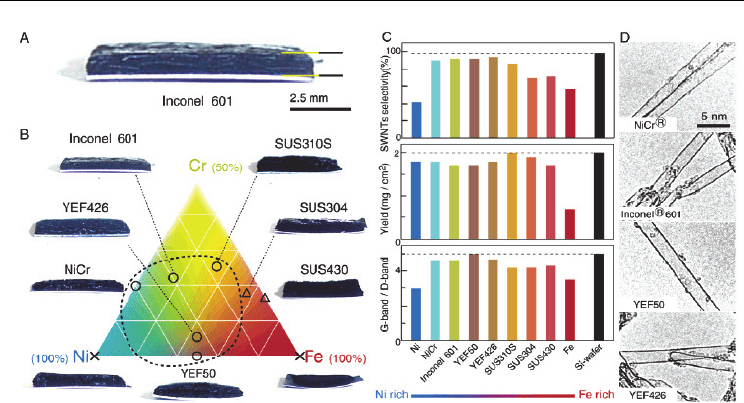
426, NiCr, YEF 50, and SUS 310S, covering a wide range of Ni-Fe-Cr compositions, as
shown in Fig. 1 (Hiraoka, 2006). Apart from the chemical compostion of substrate,
pretreatment of the alloy substrates, especially for that no any other catalyst introduced,
significantly affected the efficiency of CNT growth on the metallic substrates. It was
reported that surface roughness variation of the alloy by polishing might change the
surface chemistry, resulting in inhomogeneous growth of CNTs (Oye, et al. 2010).
Direct Growth of Carbon Nanotubes on Metal Supports by Chemical Vapor Deposition
101
Fig. 1. Direct growth of CNT forests on Ni-Cr-Fe alloys with water-assisted CVD. (A) A
photograph of a SWNT forest synthesized on Inconel 601. (B) Correlation between
components of Ni-Cr-Fe alloys and photographs of CNT forests grown on them. Symbols
indicate the level of SWNT selectivity (O high selectivity; ≥ medium selectivity; ⋅ low
selectivity). (C) A family of histograms showing selectivity of SWNTs, yield per cm
2
, and G-
band/D-band ratio of Raman spectra. (D) TEM images of SWNTs synthesized on Ni-based
alloys. (Hiraoka, 2006)
2.2 Other metals as substrates
In current electrical and electronic industries, Cu is the most popular raw material due to
their high electric and thermal conductivity with relatively low cost. Thus, it is very
interesting to directly grow CNTs on Cu substrate. It is known that Cu can act as effective
catalyst for CNT growth under certain conditions (Gan, et al. 2001 & Qin, et al. 2004).
However, the grown carbon nanostructures catalyzed by Cu are spaghetti-like and the
catalytic activity of copper is accepted to be much lower than Fe, Co and Ni (Zhang, 2010).
Therefore, it seems necessary to introduce other more active catalyst to grow dense aligned
CNTs on copper substrate. Directly deposition of catalyst on Cu substrate is an obvious
choice. However, as discussed above, Cu is not an efficient catalyst for CNT growth and
easy to form a solid solution with the common catalysts (especially for Ni) at high
temperature. The diffusion between catalyst and copper substrate may induce the loss of
catalyst. Thus, the catalyst layer should be thick enough to guarantee enough unaffected
catalyst residues to catalyze CNT growth (Singh, 2002 & Yin, 2008), meanwhile, some
authors reported that thicker catalyst layers resulted in larger diameter of grown CNTs
(Atthipalli, 2011). Therefore, adding a diffusion barrier layer between catalyst and copper
substrate is a promising and preferable choice for high-quality aligned CNT growth,
although this may increase the contact resistance between CNTs and Cu substrate in some
content. A thin layer of alumina has been used as diffusion barrier in most literatures. Lin et
al. investigated the effect of the deposition method and thickness of alumina layer on the
quality of CNT growth systematically, infering that a well-controlled conformal alumina

Carbon Nanotubes - Synthesis, Characterization, Applications
102
support layer played an important role for the aligned CNT growth with high quality and
reproducibility (Lin, et al., 2010). Other ceramic materials, such as TiN, In
2
O
3
:Sn (ITO), and
SiN
x
, were also examined as effective barrier, inferring that the extent of CNT coverage
depended on the barrier layer quality (Garcı´a-Ce´spedes, et al., 2009). Apart from ceramic
materials, some metals, such as Ti (Sung, et al., 2008), Cr, Au, Ta (Nessim, et al., 2009 &
2010), Pa (Nessim, et al., 2010), Al (Burt, et al., 2009 & Kavian, et al., 2011), and so on (Wang,
et al., 2003 & Kim & Gangloff, 2009), were also used as efficient barrier layers or substrates
directly. Although CNT growth on these substrates or underlayers was affected by many
factors, understanding the coupled influences of barrier layer thickness, grain size, and
catalyst dewetting is an important step in development of a more complete understanding
of CNT growth mechanisms.
2.3 Applications of CNTs directly grown on bulk metal substrate
Due to a high aspect ratio geometry, small tip radius, good chemical stability, low coefficient
of thermal expansion, high thermal and electrical conductivity and mechanical strength,
CNTs have attracted great interest as thermal management materials for microelectronic
packaging, electrode materials for use in energy storage cells and supercapacitors, field
emission (FE) electron sources for use in flat panel displays, e-beam lithography equipment,
x-ray sources, and vacuum microwave amplifiers, and so on. For these applications, as
discussed above, high electrical and thermal conductivities are required, which usually
needs a conductive substrate to connect with CNTs. Compared with the external
connections, the biggest benefit for direct growth technique of CNTs on metal substrate is
that can reduce the contact resistance and form an ohmic connection between CNTs and
metal substrate, which is crucial for electronic devices. Thus, it is expected to have a
significant advance toward the goal of replacing external metal conections with CNTs, such
as CMOS-compatible processes, by direct growth technique (Nessim, et al., 2009 & Kim, et
al., 2010). Experimental results indicated electrical contact through the CNT carpet to the
metallic substrate (Cu) by direct growth with an approximate resistance of 35 kΩ for
multiwall CNT carpets taller than two micrometers (Nessim, 2009). Talapatra et al. further
certified that the average total contact resistance of aligned CNTs directly grown on inconel
by a vapour-phase catalyst delivery CVD method, measured over many samples (typical
pattern size = 70μm×70μm, height=50μm), was even as low as about 500Ω. The power
density for the double-layer capacitors fabricated using the Inconel substrate with directly
grown aligned nanotubes as electrodes was about 7 kW kg
-1
even at a high scan rate of 1000
mV s
-1
(Talapatra, et al., 2006). Due to the good bonding and excellent conductivity by
interface-controlled growth of CNTs directly on Cu current collectors, Li ion battery using
the novel directly grown binder-free CNTs structure as anode showed very high specific
capacity, almost three times as that of graphite, excellent rate capability even at a
charging/discharging rate of 3 C, and no capacity degradation up to 50cycles (Lahiri, ea al.,
2010). The CNT-based field emitters, prepared on metallic substrates by direct thermal
chemical vapor deposition, exhibited a very low turn-on field, high emission current, long
time stability and good resistance to degradation in high-field, long-time exposure (Mauger,
et al., 2004 & Sung, et al., 2008 & Mahanandia, et al., 2009 & Yi & Yang, 2010 & Li, et al.,
2010 & Lahiri, et al, 2010). Furthermore, Zhang, et al. indicated that coiled carbon
nanosturctures with more defects by direct growth exhibited better field emission properties

Direct Growth of Carbon Nanotubes on Metal Supports by Chemical Vapor Deposition
103
than straight CNTs (Zhang, et al., 2010). Several studies have revealed that CNTs have
unusually high thermal conductivity in their axial direction (Berber, et al., 2000 & Kim, et al.,
2010). Thus, one promising application of CNTs in microelectronics is to use vertically
aligned CNT arrays as novel thermal interface materials (TIMs). Direct synthesis of
vertically aligned CNT TIM layer on the backside of a silican chip is not compatible with
current electronic packaging systems. Instead vertically aligned CNT synthesis on metallic
substrate, especially for copper, is preferred. The TIM, made up of a thin copper foil covered
with Cr-Au-MWCNT on both sides, showed a thermal resistance as low as 12 mm
2
K/W
(Wang, et al., 2007). Recently, Lin, et al. developed a novel assembling process of
incorporating carbon nanotubes as TIM for heat dissipation by synthesizing vertically
aligned CNTs on a copper substrate and chemically bonding the carbon nanotubes to a
silicon surface. Experimental results indicated that such an interface modification improved
the effective thermal diffusivity of the carbon nanotube-mediated thermal interface by an
order of magnitude and conductivity by almost two orders of magnitude (Lin, et al., 2010).
Due to the retained mechanical flexibility of the metallic substrate (such as stainless steel)
after CNT forest synthesis and its renewability and low cost, direct growth of CNTs on
metallic substrate becomes a promising approach for industrial production of CNTs, CNT
yarns and sheets (Baddour, et al., 2010 & Lepro´, et al., 2010 & Iijima, 2011).
3. Direct growth of CNTs on metal powders
Since their discovery, carbon nanotubes have been regarded as an ideal reinforcement for
composites to overcome the performance limits of conventional materials, due to their
excellent mechamical and physical properties. Many research efforts have dealt with
CNT/polymer composites, which exhibit a tremendous strengthening effect for the
composites (García, et al., 2007). However, the results in metals are not as encouraging as
those in polymer. This is mainly due to the difficulties in achieving homogeneous dispersion
of CNTs in metal matrix and good interfacial bonding between CNTs and metal matrix. So
far, nearly all the efforts were made through powder metallurgy route, which involved
Fig. 2. Schematic diagram of the CNT growth directly on metal powders
NaOH solution
Metal powders
☆Catalyst
element salt
solution
Colloid
solution
*Constant
stirring
Catalyst
precursor
Drying
Calcining
Catalyst
CNT growth on metal
powder
Reducing by H
2
☆For Ni catalyst, the catalyst element salt is Ni(NO
3
)
2
•6H
2
O; For Ni/Y catalyst, the catalyst
element salt is a mixture of Ni(NO
3
)
2
•6H
2
O and Y(NO
3
)
3
•6H
2
O
*For Mg supported catalyst, metal powders mixed with NaOH solution firstly. The salt
solution was added to the mixed solution dropwise under constant stirring
CV

Carbon Nanotubes - Synthesis, Characterization, Applications
104
mixing of CNTs with metal powders by ball milling or chemical process (Cha, et al., 2005 &
Kim, et al., 2006). In the above methods, CNTs was inclined to be damaged and lose their
initial properties during the mechanical milling or their functionalization process.
Alternatively direct synthesis of CNTs in metal matrix composites may overcome the
problems associated with conventional methods and achieve homogeneous distribution of
CNTs and good interfacial bonding between CNTs and metal matrix. In this section, we will
summarize our recent progress in this field. Several metal powders, such as Al, Cu, Mg, Ag,
have been proved as effective support for CNT growth. The catalyst dispersed on these
metal powders was prepared by deposition-precipitation. The experimental procedure was
described in Fig. 2. CNT growth was performed by a simple CVD process.
3.1 Aluminum powder
As mentioned above, aluminum can be used as effective underlayer or substrate for catalyst
deposition, probably due to its easy formation of a passivation oxide layer on the surface of
Al (Liu, et al., 2008). In our study, Ni nanoparticles were homogeneously deposited on Al
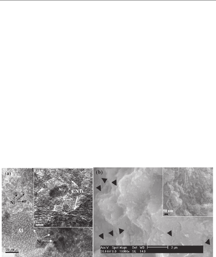
particle surface by a direct deposition-precipitation method. Fig. 3 displays transmission
electron microscopy (TEM) images of representative Ni–Al catalyst powders. Almost all Al
powders are evenly decorated by several Ni nanoparticles. It is found that catalytic particles
of different sizes can be formed by varying the reduction temperature, which thus controls
the diameter of the growing tubes. When reducing the catalyst precursor at 400 °C for 2 h,
the diameter of the Ni particles ranged from 5 to 20 nm. It can be clearly seen from Figure 3b
that Ni nanoparticles with even diameters are homogeneously dispersed on the surface of
the Al powders.
Fig. 3. Microstructures of the Ni–Al catalyst powders, in which the Ni nanoparticles with a
narrow diameter distribution are homogeneously dispersed on the surface of the Al
powder. a) TEM image of a Ni–Al catalyst powder, obtained by reducing the catalyst
precursor at 400℃ for 2 h (scale bar: 50 nm). b) TEM image of a Ni–Al catalyst powder,
showing that the gray Al powder is evenly decorated by several black Ni nanoparticles
(scale bar: 50 nm).
Direct Growth of Carbon Nanotubes on Metal Supports by Chemical Vapor Deposition
105
Fig. 4. a) Scanning electron microscopy (SEM) image of a CNT(Ni)–Al composite powder
(scale bar: 100 nm). b) Enlarged SEM image of several typical CNTs (indicated by arrows)
dispersed in the Al powders, the locations indicated with ellipses show the network
structures between CNTs and Al powders (scale bar: 50 nm). c) Low-magnification HRTEM
image of a CNT–Al composite powder (scale bar: 50 nm). d) High-resolution TEM (HRTEM)
image of a typical CNT, showing a well-graphitized multiwalled nanotube (scale bar: 5 nm).
Fig. 4a shows a low-magnification scanning electron microscopy (SEM) image of
homogeneously dispersed CNTs within the Al powders. The surfaces of the walls of the as-
grown CNTs are clean, and their diameters range from 5 to 25 nm. In addition, metallic
nanoparticles are visible at the tips of the CNTs. The most important feature of our process
is that the CNTs are synthesized into the Al powders in situ. The morphology of the
CNT(Ni)–Al powders shows an ideal composite microstructure, displaying spherical
morphologies with CNTs homogeneously dispersed into the powders. It is also found that
the density and length of the CNTs, or the CNT content of the composite powders, can be
tuned by adjusting the experimental parameters, such as the growth time and the Ni content
in the Ni–Al catalyst. With a shorter time and lower Ni content, shorter and sparser CNTs
can be obtained in the Al powders. Figure 4b is an enlarged SEM image of several typical
CNTs (indicated by arrows) dispersed in the Al powders. It can be distinctly observed that
the CNTs are not agglomerated at all. Moreover, we have noticed that some locations,
marked with ellipses in Figure 4b, form network structures between the CNTs and the Al
powders.
Carbon Nanotubes - Synthesis, Characterization, Applications
106
The microstructure details of the CNT(Ni)–Al composite powders were investigated with
high-resolution TEM (HRTEM). The low-magnification HRTEM image in Figure 4c further
verifies that the tips of the CNTs encapsulate metallic particles. An HRTEM image of a
typical CNT, as seen in Figure 4d, demonstrates that the CNTs are well-graphitized
multiwalled nanotubes. The graphitic sheets of the CNTs (see Fig. 4d) are apparent, and the
interlayer spacing between the sheets is 0.34 nm, consistent with the ideal graphitic
interlayer space (0.34 nm). To determine the length of the as-grown CNTs, dilute nitric acid
was used to remove the Al from the composite powders. TEM analysis indicates that the
CNTs are easily entangled after removing Al as a result of strong van der Waals forces
between them, and their lengths range from 1500 to 2500 nm.
The CNT(Ni)-Al bulk composite was prepared by pressing and sintering the CNT(Ni)
composite powders directly. The microstructure of the composite was investigated by TEM.
In the low magnification TEM image of Figure 5a, we see only some black Ni nanoparticles
(indicated by arrows) distributed evenly within the Al grains. When investigating the area
around the black Ni nanoparticles in detail by high-magnification TEM, it is found that the
CNTs with encapsulated Ni nanoparticles are dispersed very homogeneously within the Al
matrix (as seen in the inset of Fig. 5a). In particular, the TEM image (Fig. 5a, inset) shows
that the interfaces of the CNTs and Al bond well, and that no reactant is formed by the
present technique. Furthermore, the Al grains reinforced by CNTs present a very low
location density. Figure 5b is an SEM image of the composite fracture surface, which shows
CNTs with an obviously tubular structure (Fig. 5b, inset). Moreover, it can be observed that
the CNTs are dispersed very well into the Al matrix, and some CNTs are pulled-out or
broken (marked with triangles), which indicates that the load transfer from the matrix to the
nanotubes is sufficient to fracture the nanotubes.
Fig. 5. a) TEM image of a CNT(Ni)–Al matrix bulk composite, showing the homogeneously
dispersed CNT(Ni) within the Al matrix (scale bar: 50 nm, scale bar of inset: 5 nm). b) SEM
image of the fractured surface of a CNTs(Ni)–Al matrix bulk composite, showing the
existence of pulled-out and broken CNTs (scale bar of inset: 50 nm).
Table 1 presents a comparative study of hardness and tensile strength values of the
composite and two other typical materials that were fabricated by the same procedure (i.e.,
pressing, sintering, and re-pressing). The density of the CNT(Ni)–Al bulk composite (c) was