Neamen D. Microelectronics: Circuit Analysis and Design
Подождите немного. Документ загружается.

1288 Part 3 Digital Electronics
off. Note that when the output is low, with
Q
2
and
Q
o
in saturation, the voltage at the
base of
Q
4
is approximately 0.9 V, which is sufficient to bias
Q
4
in its active region.
However, the voltage at the emitter of
Q
4
is only approximately 0.2 V, which means that
the current in
Q
4
is very small and does not add significantly to the power dissipation.
Tristate Output
The output impedances of the totem-pole output TTL logic circuits considered thus far
are extremely low when the output voltage is in either the high or low state. In memory
circuit applications, situations arise in which the outputs of many TTL circuits must be
connected together to form a single output. This creates a serious loading situation,
demanding that all other TTL outputs be disabled or put into a high impedance state, as
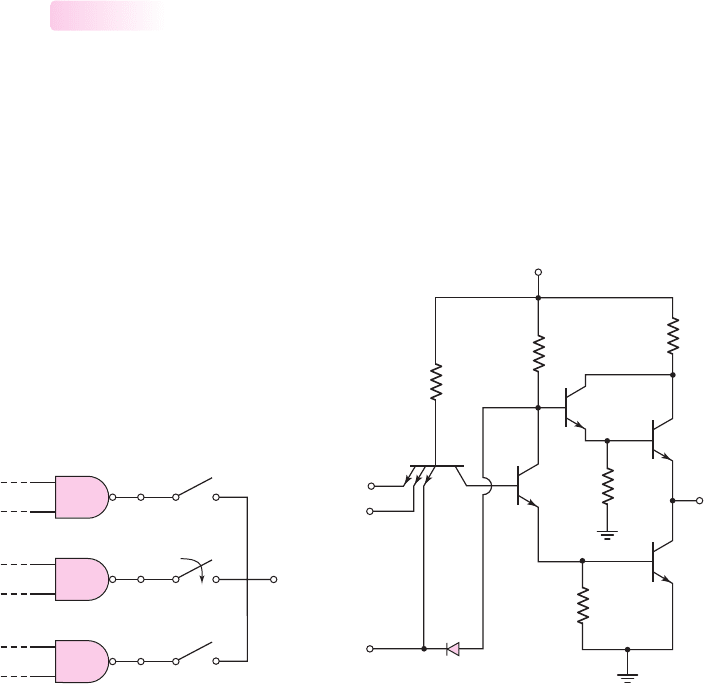
shown symbolically in Figure 17.28. Here,
G
1
and
G
3
are disconnected from the out-
put; the output voltage
v
O
then measures only the output of logic gate
G
2
.
17.3.5
v
O3
S
3
v
O2
v
O
S
2
v
O1
S
1
G
1
G
2
G
3
Figure 17.28 Circuit symbolically
showing tristate output
v
X
v
Y
V
CC
= 5.0 V
v
O
R
2
R
B
Q
2
D
2
D
Q
3
Q
o
Q
4
Q
1
R
1
R
3
R
4
–
Figure 17.29 TTL circuit with tristate output stage
The TTL circuit in Figure 17.29 may be used to put the logic output into a high
impedance state. When
¯
D = 5
V, the state of input transistor
Q
1
is controlled by
inputs
v
X
and
v
Y
. Under these circumstances, diode
D
2
is always reverse biased and
the circuit function is the NAND function already considered.
When
¯
D
is driven to a logic 0 state of 0.1 V, the low voltage at the emitter of
Q
1
ensures that both
Q
2
and
Q
o
are cut off, and the low voltage applied to
D
2
means that
D
2
is forward biased. The voltage at the base of
Q
4
is approximately 0.8 V, which
means that
Q
3
is also cut off. In this condition, then, both output transistors
Q
3
and
Q
o
are cut off. The impedance looking back into transistors that are cut off is
normally in the megohm range. Therefore, when TTL circuits are paralleled to
increase the capability of a digital system, the tristate output stage is either enabled
or disabled via the
¯
D
select line. The output stage on only one TTL circuit may be
enabled at any one time.
nea80644_ch17_1255-1314.qxd 8/6/09 11:12 AM Page 1288 pmath DATA-DISK:Desktop Folder:UDAYVEER/Neamen:

Chapter 17 Bipolar Digital Circuits 1289
Test Your Understanding
TYU 17.5 The DTL circuit in Figure 17.20 has new circuit parameters of
R
1
= 15
k
,
R
C
= 6
k
, and
R
B
= 15
k
. Assume
β = 30
for the transistor. Deter-
mine
i
1
,
i
2
,
i
R
,
i
B
,
i
RC
, and
v
O
for: (a)
v
X
= v
Y
= 0.1
V; (b)
v
X
= 5
V,
v
Y
= 0.1
V;
and (c)
v
X
= v
Y
= 5
V. (Ans. (a)
i
1
= 0.28
mA,
i
2
= i
R
= i
B
= i
RC
= 0
,
v
O
= 5
V;
(b) Same as part (a); (c)
i
1
= i
2
= 0.1867
mA,
i
R
= 0.0533
mA,
i
B
= 0.1334
mA,
i
RC
= 0.8167
mA,
v
O
= 0.1
V)
TYU 17.6 For the basic DTL logic circuit in Figure 17.20, the parameters are the same
as given in Exercise TYU 17.5. (a) Calculate the maximum fanout for the low output
condition such that
Q
o
remains in saturation. (b) Repeat part (a) for the condition that
the maximum rated collector current is
I
C,max
= 12
mA. (Ans. (a)
N = 9
, (b)
N = 9
)
TYU 17.7 Consider the TTL circuit shown in Figure 17.24 with parameters as given
in Exercise Ex 17.9. Calculate the maximum fanout for the low output. For the low
output condition, assume that the output transistor must remain in saturation. (Ans.
N = 63
)
TYU 17.8 For the tristate TTL circuit in Figure 17.29, the parameters are:
R
1
=
6k
,
R
2
= 2k
,
R
3
= 100
,
R
4
= 4k
, and
R
B
= 1k
. Assume that
β
F
≡
β = 20
and
β
R
= 0.1
(for each input emitter). For
¯
D = 0.1
V, calculate the base and
collector currents in each transistor. (Ans.
i
B1
= 0.683 mA
,
|i
C1
|=i
B2
= i
C2
=
i
Bo
= i
Co
= 0
,
i
B4
= 1.19 μA
,
i
C4
= 23.8 μA
,
i
B3
= i
C3
= 0
)
17.4 SCHOTTKY TRANSISTOR–TRANSISTOR LOGIC
Objective: • Analyze and design Schottky and low-power Schottky
transistor–transistor logic circuits
The TTL circuits considered thus far drive the output and phase-splitter transistors
between cutoff in the high output state and saturation in the low output state. The
input transistor is driven between saturation and the inverse-active mode. Since the
propagation delay time of a TTL gate is a strong function of the storage time of
the saturation transistors, a nonsaturation logic circuit would be an advantage. In the
Schottky clamped transistor, the transistor is prevented from being driven into deep
saturation and has a storage time of only approximately 50 ps.
Schottky Clamped Transistor
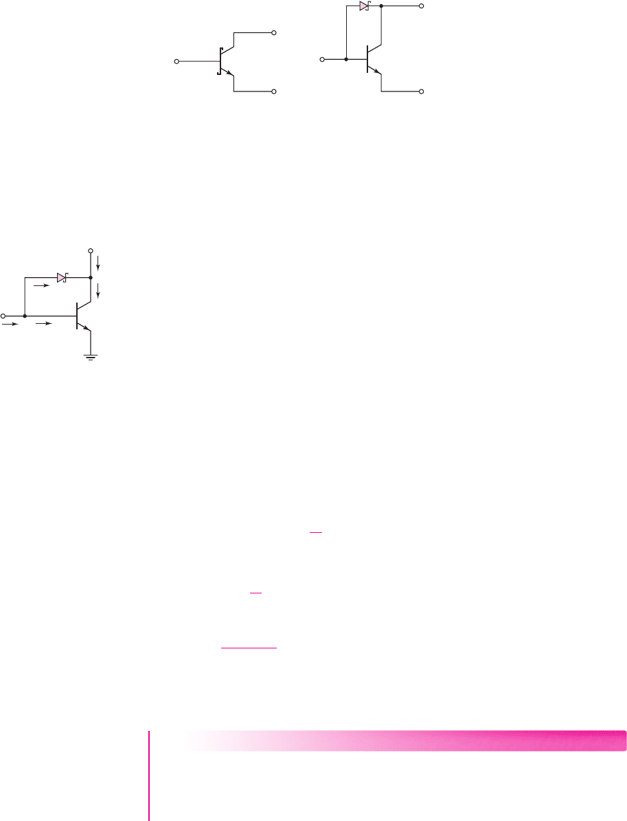
The symbol for the Schottky clamped transistor, or simply the Schottky transistor, is
shown in Figure 17.30(a); its equivalent configuration is given in Figure 17.30(b).
In this transistor, a Schottky diode is connected between the base and collector of an
npn bipolar transistor. Two characteristics of the Schottky diode are: a low turn-on
voltage and a fast-switching time. When the transistor is in its active region, the base–
collector junction is reverse biased, which means that the Schottky diode is reverse
biased and effectively out of the circuit. The Schottky transistor then behaves like a
normal npn bipolar transistor. As the Schottky transistor goes into saturation, the
17.4.1
nea80644_ch17_1255-1314.qxd 8/6/09 11:12 AM Page 1289 pmath DATA-DISK:Desktop Folder:UDAYVEER/Neamen:
1290 Part 3 Digital Electronics
base–collector junction becomes forward biased, and the base–collector voltage is
effectively clamped at the Schottky diode turn-on voltage, which is normally between
0.3 and 0.4 V. The excess base current is shunted through the diode, and the basic npn
transistor is prevented from going deeply into saturation.
Figure 17.31 shows the equivalent circuit of the Schottky transistor with desig-
nated currents and voltages. Currents
i
C
and
i
B
are the collector and base currents,
respectively, of the Schottky transistor, while
i
C
and
i
B
are the collector and base
currents, respectively, of the internal npn transistor.
The three defining equations for the Schottky transistor are
i
C
= i
D
+i
C
(17.18)
i
B
= i
B
+i
D
(17.19)
and
i
C
= βi
B
(17.20)
Equation (17.20) is appropriate since the internal transistor is clamped at the
edge of saturation. If
i
C
<βi
B
, then the Schottky diode is forward biased,
i
D
> 0
,
and the Schottky transistor is said to be in saturation. However, the internal transis-
tor is only driven to the edge of saturation in this case.
Combining Equations (17.19) and (17.20), we find that
i
D
= i
B
−i
B
= i
B
−
i
C
β
(17.21)
Substituting this equation into Equation (17.18) yields
i
C
= i
B
−
i
C
β
+i
C
(17.22(a))
or
i
C
=
i
B
+i
C
1 + (1/β)
(17.22(b))
Equation (17.22(b)) relates the internal transistor collector current to the external
Schottky transistor collector and base currents.
EXAMPLE 17.11
Objective: Determine the currents in a Schottky transistor.
Consider the Schottky transistor in Figure 17.31 with an input base current of
i
B
= 1mA
. Assume that
β = 25
. Determine the internal currents in the Schottky
transistor for
i
C
= 2mA
, and then for
i
C
= 20 mA
.
B
C
E
B
C
E
(a) (b)
Figure 17.30 (a) Schottky clamped transistor symbol
and (b) Schottky clamped transistor equivalent circuit
+
+
–
–
i
D
i
C
′
i
B
′
i
C
i
B
v
CE
v
BE
v
D
+
–
Figure 17.31 Schottky
clamped transistor equivalent
circuit, with currents and
voltages
nea80644_ch17_1255-1314.qxd 8/6/09 11:12 AM Page 1290 pmath DATA-DISK:Desktop Folder:UDAYVEER/Neamen:

Chapter 17 Bipolar Digital Circuits 1291
Solution:
For
i
C
= 2mA
, the internal collector current is, from Equation (17.22(b)),
i
C
=
1 + 2
1 + (1/25)
= 2.885 mA
and the internal base current is
i
B
=
i
C
β
=
2.885
25
= 0.115 mA
The Schottky diode current is therefore
i
D
= i
B
−i
B
= 1 −0.115 = 0.885 mA
Repeating the calculations for
i
C
= 20 mA
, we obtain
i
C
= 20.2mA
i
B
= 0.808 mA
i
D
= 0.192 mA
Comment: For a relatively small collector current into the Schottky transistor, the
majority of the input base current is shunted through the Schottky diode. As the
collector current into the Schottky transistor increases, less current is shunted through
the Schottky diode and more current flows into the base of the npn transistor.
EXERCISE PROBLEM
Ex 17.11: Consider the Schottky clamped transistor in Figure 17.32. Assume
β = 15
,
V
BE
(on) = 0.7
V and
V
γ
(SD) = 0.3
V. (a) For no load,
i
L
= 0
, find the
currents
i
D
,
i
B
, and
i
C
. (b) Repeat part (a) for a load current of
i
L
= 10
mA. (c) De-
termine the maximum load current
i
L
that the load transistor can sink and still remain
at the edge of saturation. (Ans. (a)
i
C
= 3.791
mA,
i
B
= 0.253
mA,
i
D
= 1.747
mA;
(b)
i
C
= 13.166
mA,
i
B
= 0.878
mA,
i
D
= 1.122
mA; (c)
i
L
∼
=
28
mA)
Since the internal npn bipolar transistor is not driven deeply into saturation, we
assume that the B–E junction voltage remains equal to the turn-on voltage, or
v
BE
=
V
BE
(on)
. If the Schottky transistor is biased in saturation, then the C–E voltage is
v
CE
= V
CE
(sat) = V
BE
(on) − V
γ
(SD)
(17.23)
where
V
γ
(SD)
is the turn-on voltage of the Schottky diode. Assuming parameter
values of
V
BE
(on) = 0.7V
and
V
γ
(SD) = 0.3
V, the collector–emitter saturation
voltage of a Schottky transistor is
V
CE
(sat) = 0.4V
. When the Schottky transistor is
at the edge of saturation, then
i
D
= 0
,
i
C
= βi
B
, and
v
CE
= V
CE
(sat)
.
Schottky TTL NAND Circuit
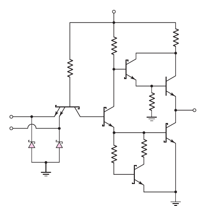
Figure 17.33 shows a Schottky TTL NAND circuit in which all of the transistors
except
Q
3
are Schottky clamped transistors. The connection of
Q
4
across the
base–collector of
Q
3
prevents this junction from becoming forward biased, ensuring
that
Q
3
never goes into saturation. Another difference between this circuit and the
standard TTL circuit is that the pull-down resistor at the base of output transistor
Q
o
has been replaced by transistor
Q
5
and two resistors. This arrangement is called a
17.4.2
i
D
i
B
= 2 mA
i
L
R
C
= 2.25 kΩ
V
CC
= 5 V
i
C
′
i
B
′
Figure 17.32 Figure for
Exercise Ex 17.11
nea80644_ch17_1255-1314.qxd 8/6/09 11:12 AM Page 1291 pmath DATA-DISK:Desktop Folder:UDAYVEER/Neamen:
1292 Part 3 Digital Electronics
squaring network, since it squares, or sharpens, the voltage transfer characteristics
of the circuit.
Device
Q
2
is prevented from conducting until the input voltage is large enough
to turn on both
Q
2
and
Q
o
simultaneously. Recall that the passive pull-down resistor
on the TTL circuit provided a pathway for removing stored charge in the base of the
output transistor, when the output transistor was turned off from the saturated state.
Transistor
Q
5
now provides an active pull-down network that pulls
Q
o
out of satura-
tion more quickly.
This is one example of a circuit in which the piecewise linear model of a tran-
sistor fails to provide an adequate solution for the circuit analysis. With the piecewise
linear model,
Q
5
would apparently never turn on. However, because of the exponen-
tial relationship between collector current and base-emitter voltage, transistor
Q
5
does turn on and does help pull
Q
o
out of saturation during switching.
The two Schottky diodes between the input terminals and ground act as clamps
to suppress any ringing that might occur from voltage transitions. The input diodes
clamp any negative undershoots at approximately
−0.3
V.
The dc current–voltage analysis of the Schottky TTL circuit in Figure 17.33 is
similar to that for the standard TTL circuit. One minor difference is that when the
inputs are high and the input transistor is in the inverse-active mode, the B–C
forward bias voltage is 0.3 V, because of the Schottky diode connected between the
base and collector junctions.
The major difference between the Schottky circuit and standard TTL circuits is
the quantity of excess minority carrier storage in the transistors when they are driven
into or near saturation. The internal npn transistor of the Schottky clamped transistor
is held at the edge of saturation, and the resulting propagation delay time is on the
order of 2 to 5 ns, compared to a nominal 10 to 15 ns for standard TTL circuits.
A slight difference between the Schottky and standard TTL circuits is the value
of the output voltage in the logic 0 state. The low output voltage of a standard TTL
circuit is in the range of 0.1 to 0.2 V, while the Schottky transistor low output
V
CC
= 5 V
R
1
=
2.8 kΩ
R
4
=
3.5 kΩ
R
5
=
370 Ω
R
2
= 760 Ω
Q
4
Q
2
Q
5
Q
1
Q
3
R
3
= 55 Ω
R
6
=
350 Ω
v
O
v
X
v
Y
Q
o
Figure 17.33 Schottky TTL NAND logic circuit
nea80644_ch17_1255-1314.qxd 8/6/09 11:12 AM Page 1292 pmath DATA-DISK:Desktop Folder:UDAYVEER/Neamen:
Chapter 17 Bipolar Digital Circuits 1293
saturation voltage,
V
OL
, is approximately 0.4 V. The output voltage in the logic 1
state is essentially the same for both types of logic circuits.
Low-Power Schottky TTL Circuits
The Schottky TTL circuit in Figure 17.33 and the standard TTL circuit dissipate
approximately the same power, since voltage and resistance values in the two circuits
are similar. The advantage of the Schottky TTL circuit is the reduction in propagation
delay time by a factor of 3 to 10.
Propagation delay times depend on the type of transistors (Schottky clamped or
regular) used in the circuit, and on the current levels in the circuit. The storage time
of a regular transistor is a function of the reverse base current that pulls the transistor
out of saturation. Also, the transistor turn-on time depends on the current level charg-
ing the base–emitter junction capacitance. A desirable trade-off can therefore be made
between current levels (power dissipation) and propagation delay times. Smaller
current levels lead to lower power dissipation, but at the expense of increased prop-
agation delay times. This trade-off has been successful in commercial applications,
where very short propagation delay times are not always necessary, but reduced
power requirements are always an advantage.
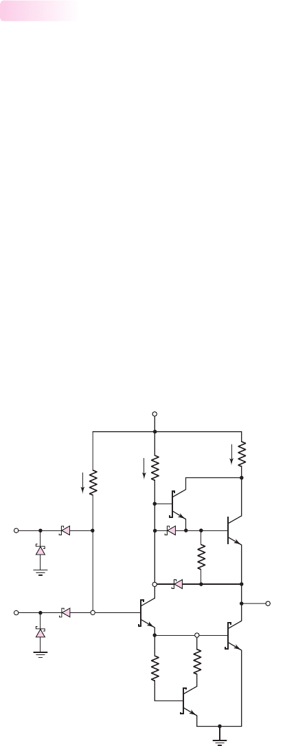
A low-power Schottky TTL NAND circuit is shown in Figure 17.34. With few
exceptions, these circuits do not use the multiemitter input transistor of standard TTL
circuits. Most low-power Schottky circuits use a DTL type of input circuit, with
Schottky diodes performing the AND function. This circuit is faster than the classic
multiemitter input transistor circuit, and the input breakdown voltage is also higher.
The dc analysis of the low-power Schottky circuit is identical to that of DTL
circuits.
17.4.3
V
CC
= 5 V
R
1
=
20 kΩ
R
5
= 1.5 kΩ
R
2
= 8.0 kΩ
Q
4
D
5
D
4
D
2
D
3
D
1
D
6
Q
2
Q
5
R
3
=
120 Ω
R
6
=
3.0 kΩ
R
4
=
4.0 kΩ
v
O
v
BO
v
C2
v
1
v
Y
v
X
Q
o
Q
3
i
2
i
3
i
1
Figure 17.34 Low-power Schottky TTL NAND logic circuit
nea80644_ch17_1255-1314.qxd 8/6/09 11:12 AM Page 1293 pmath DATA-DISK:Desktop Folder:UDAYVEER/Neamen:

1294 Part 3 Digital Electronics
EXAMPLE 17.12
Objective: Calculate the power dissipation in a low-power Schottky TTL circuit.
Consider the circuit shown in Figure 17.34. Assume the Schottky diode turn-on
voltage is
V
γ
(SD) = 0.3
V and the transistor parameters are:
V
BE
(on) = 0.7V
,
V
CE
(sat) = 0.4V
, and
β = 25
.
Solution: For the low input condition,
v
X
= v
Y
= 0.4V
and
v
1
= 0.4 +0.3 =
0.7V
. Current
i
1
is
i
1
=
V
CC
−v
1
R
1
=
5 − 0.7
20
= 0.215 mA
Since
Q
2
and
Q
o
are cut off with a no-load condition, all other currents in the circuit
are zero. The power dissipation for the low input condition is therefore
P
L
= i
1
(V
CC
−v
X
) = (0.215) · (5 −0.4) = 0.989 mW
For the high input condition,
v
X
= v
Y
= 3.6V
, voltage
v
1
is
v
1
= V
BE
(on)
Q
o
+ V
BE
(on)
Q
2
= 0.7 +0.7 = 1.4V
and voltage
v
C2
is
v
C2
= V
BE
(on)
Q
o
+ V
CE
(sat)
Q
2
= 0.7 +0.4 = 1.1V
The currents are then
i
1
=
V
CC
−v
1
R
1
=
5 − 1.4
20
= 0.18 mA
and
i
2
=
V
CC
−v
C2
R
2
=
5 − 1.1
8
= 0.488 mA
When
v
C2
= 1.1V
and
v
O
= 0.4V
, transistor
Q
4
is at the edge of turn-on, how-
ever, since there is no voltage drop across
R
4
,
Q
4
has negligible emitter current. For
a no-load condition, all other currents are zero. Therefore, the power dissipation for
the high input condition is
P
H
= (i
1
+i
2
)V
CC
= (0.18 +0.488) ·5 = 3.34 mW
Comment: The power dissipation in this low-power Schottky TTL circuit is approxi-
mately a factor of five smaller than in the Schottky or standard TTL logic gates. The
propagation delay time in the low-power Schottky circuit is approximately 10 ns,
which compares closely with the propagation delay time for a standard TTL circuit.
EXERCISE PROBLEM
Ex 17.12: Assume the low-power Schottky TTL circuit in Figure 17.34 is
redesigned such that
R
1
= 40 k
and
R
2
= 12 k
, and all other circuit parame-
ters remain the same. The transistor and diode parameters are:
V
BE
(on) = 0.7V
,
V
CE
(sat) = 0.4V
,
β = 25
, and
V
γ
(SD) = 0.3
V. Assuming no load, determine
the base and collector currents in each transistor, and the power dissipation in the
gate, for: (a)
v
X
= v
Y
= 0.4V
, and (b)
v
X
= v
Y
= 3.6V
. (Ans. (a)
i
B2
=
i
C2
= i
Bo
= i
Co
= i
B5
= i
C5
= 0
,
i
B3
= i
C3
= i
B4
= i
C4
= 0
,
P = 495 μW
(b)
i
B2
= 90 μA
,
i
C2
= 325 μA
,
i
B4
= i
C4
= i
B3
= i
C3
= 0
,
i
B5
∼
=
i
C5
∼
=
0
,
i
Bo
= 415 μA
,
i
Co
= 0
,
P = 2.08 mW
)
nea80644_ch17_1255-1314.qxd 8/6/09 11:12 AM Page 1294 pmath DATA-DISK:Desktop Folder:UDAYVEER/Neamen:
Chapter 17 Bipolar Digital Circuits 1295
Diodes
D
5
and
D
6
are called speedup diodes. As we showed in the dc analysis,
these diodes are reverse biased when the inputs are in either a static logic 0 or a logic 1
mode. When at least one input is in a logic 0 state, the output is high, and
Q
3
and
Q
4
tend to turn on, supplying any necessary load current. When both inputs are switched
to their logic 1 state,
Q
2
turns on and
v
C2
decreases, forward biasing
D
5
and
D
6
.
Diode
D
5
helps to pull charge out of the base of
Q
3
, turning this transistor off more
rapidly. Diode
D
6
helps discharge the load capacitance, which means that output
voltage
v
O
switches low more rapidly.
Advanced Schottky TTL Circuits
The advanced low-power Schottky circuit possesses the lowest speed–power product
with a propagation delay time short enough to accommodate a large number of digital
applications, while still maintaining the low power dissipation of the low-power
Schottky family of logic circuits. The major modification lies in the design of the input
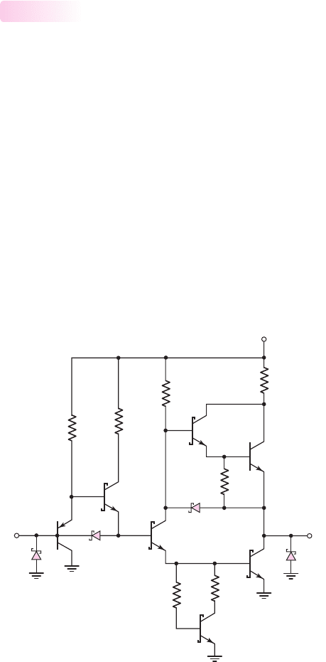
circuitry. Consider the circuit shown in Figure 17.35. The input circuit contains a pnp
transistor
Q
1
, a current amplification transistor
Q
2
, and a Schottky diode
D
2
from the
base of
Q
3
to the input. Diode
D
2
provides a low-impedance path to ground when the
input makes a high-to-low transition. This enhances the inverter switching time. The
current driver transistor
Q
1
provides a faster transition when the input goes from low
to high than if a Schottky diode input stage were used. Transistor
Q
1
provides the
switch element that steers current from
R
1
either to
Q
2
or the input source.
When
v
X
= 0.4V
, the E–B junction of
Q
1
is forward biased, and
Q
1
is biased in
its active region. The base voltage of
Q
2
is approximately 1.1 V;
Q
2
,
Q
3
, and
Q
5
are cut
off; and the output voltage goes high. Most of the current through
R
1
goes to ground
through
Q
1
, so very little current sinking is required of the driver output transistor. When
17.4.4
V
CC
= 5 V
R
1
=
40 kΩ
R
2
=
50 kΩ
R
4
=
4.0 kΩ
R
6
=
6.0 kΩ
R
5
=
3.0 kΩ
R
3
= 15 kΩ
Q
6
D
3
D
2
D
1
D
4
Q
7
Q
5
Q
4
Q
3
Q
2
Q
1
R
7
= 50 Ω
v
O
v
X
Figure 17.35 Advanced low-power Schottky (ALS) inverter gate
nea80644_ch17_1255-1314.qxd 8/6/09 11:12 AM Page 1295 pmath DATA-DISK:Desktop Folder:UDAYVEER/Neamen:

1296 Part 3 Digital Electronics
v
X
= 3.6V
, transistors
Q
2
,
Q
3
, and
Q
5
turn on, the voltage at the base of
Q
2
is clamped
at approximately 2.1 V, the E–B junction of
Q
1
is reverse biased, and
Q
1
is cut off.
With fast switching circuits, inductances, capacitances, and signal delays may
introduce problems requiring the use of transmission line theory. Clamping diodes
D
1
and
D
4
at the input and output terminals clamp any negative-going switching
transients that result from ringing signals on the interconnect lines.
Test Your Understanding
TYU 17.9 In the Schottky TTL NAND circuit in Figure 17.33, assume
β
F
≡ β = 25
and
β
R
= 0
. For a no-load condition, calculate the power dissipation for: (a)
v
X
=
v
Y
= 0.4V
, and (b)
v
X
= v
Y
= 3.6V
. (Ans.
P = 6.41 mW
(b)
P = 31.4mW
)
TYU 17.10 Consider the advanced low-power Schottky circuit in Figure 17.35.
Determine the currents in
R
1
and
R
2
for (a)
v
X
= 0.4
V and (b)
v
X
= 3.6
V. (Ans.
(a)
i
R1
= 97.5 μ
A,
i
R2
= 0;
(b)
i
R1
= 72.5 μ
A,
i
R2
= 64 μ
A)
TYU 17.11 Let
V
CC
= 3.5
V for the advanced low-power Schottky circuit in Figure
17.35. Determine the currents in
R
1
and
R
2
for (a)
v
X
= 0.4
V and (b)
v
X
= 2.1
V.
(Ans. (a)
i
R1
= 60 μ
A,
i
R2
= 0
; (b)
i
R1
= 35 μ
A,
i
R2
= 34 μ
A)
17.5 BiCMOS DIGITAL CIRCUITS
Objective: • Analyze BiCMOS digital logic circuits
As we have discussed previously, BiCMOS technology combines bipolar and CMOS
circuits on one IC chip. This technology combines the high-input-impedance, low-
power characteristics of CMOS with the high-current drive characteristics of bipolar
circuits. If the CMOS circuit has to drive a few other similar CMOS logic circuits,
the current drive capability is not a problem. However, if a circuit has to drive a
relatively large capacitive load, bipolar circuits are preferable because of the rela-
tively large transconductance of BJTs.
We consider a BiCMOS inverter circuit and then a simple example of a BiCMOS
digital circuit. This section is intended only to introduce this technology.
BiCMOS Inverter
Several BiCMOS inverter configurations have been proposed. In each case, npn
bipolar transistors are used as output devices and are driven by a quasi-CMOS
inverter configuration. The simplest BiCMOS inverter is shown in Figure 17.36(a).
The output stage of the npn transistors is similar to the totem-pole output stage of the
TTL circuits that were considered in Section 17.3.
When the input voltage
v
I
of the BiCMOS inverter in Figure 17.36(a) is low,
the transistors
M
N
and
Q
2
are cut off. The transistor
M
P
is turned on and provides
base current to
Q
1
so that
Q
1
turns on and supplies current to the load capacitance.
The load capacitance charges and the output voltage goes high. As the output voltage
goes high, the output current will normally become very small, so that
M
P
is driven
17.5.1
nea80644_ch17_1255-1314.qxd 8/6/09 11:12 AM Page 1296 pmath DATA-DISK:Desktop Folder:UDAYVEER/Neamen:

Chapter 17 Bipolar Digital Circuits 1297
into its nonsaturation region and the drain-to-source voltage will become essentially
zero. The transistor
Q
1
will essentially cut off and the output voltage will charge to
a maximum value of approximately
v
O
(max) = V
DD
− V
BE
(on)
.
When the input voltage
v
I
goes high,
M
P
turns off, eliminating any bias current
to
Q
1
, so
Q
1
is also off. The two transistors
M
N
and
Q
2
turn on and provide a
discharge path for the load capacitance so the output voltage goes low. In steady
state, the load current will normally be very small, so
M
N
will be biased in the
nonsaturation region. The drain-to-source voltage will become essentially zero. The
transistor
Q
2
will be essentially off and the output voltage will discharge to a mini-
mum value of approximately
v
O
(min)
∼
=
V
BE
(on)
.
One serious disadvantage of the inverter in Figure 17.36(a) is that there is no
path through which base charge from the npn transistors can be removed when they
are turning off. Thus, the turn-off time of the two npn transistors can be relatively
long. A solution to this problem is to include pull-down resistors, as shown in the cir-
cuit in Figure 17.36(b). Now, when the npn transistors are being turned off, the stored
base charge can be removed to ground through
R
1
or
R
2
. An added advantage of this
circuit is, that when
v
I
goes high and the output goes low, the very small output cur-
rent through
M
N
and
R
2
means the output voltage is pulled to ground potential. Also,
as
v
I
goes low and the output goes high, the very small load current means that the
output is pulled up to essentially
V
DD
through the resistor
R
1
. We may note that the
two npn output transistors are never on at the same time.
Other circuit designs incorporate other transistors that aid in turning transistors
off and increasing switching speed. However, these two examples have demonstrated
the basic principle used in BiCMOS inverter circuit designs.
BiCMOS Logic Circuit
In BiCMOS logic circuits, the logic function is implemented by the CMOS portion of
the circuit and the bipolar transistors again act as a buffered output stage providing the
17.5.2
V
DD
V
DD
M
P
M
N
v
O
v
O
v
I
v
I
Q
1
M
P
Q
1
R
1
R
2
Q
2
M
N
Q
2
(a) (b)
Figure 17.36 (a) Basic BiCMOS inverter. (b) Improved version of BiCMOS inverter.
nea80644_ch17_1255-1314.qxd 8/6/09 11:12 AM Page 1297 pmath DATA-DISK:Desktop Folder:UDAYVEER/Neamen:
