Messerschmidt U. Dislocation Dynamics During Plastic Deformation
Подождите немного. Документ загружается.

212 6 Semiconductors
1 µm
(a)
a
a
b
b
1 µm
[–110]
[01–1]
1
2
a
a'
(b)
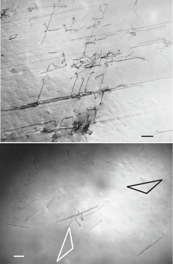
Fig. 6.4. Dislocation structures in Si-5 at% Ge taken during an in situ straining
experiment in the partly unloaded state. (a) 610
◦
C, (b) 745
◦
C. From the work in
[368]
6.3 Dislocation Dynamics 213
In summarizing, it may be stated that dislocations arrange along the
Peierls valleys at rest and during the motion at low temperatures, that is,
at high stresses. 60
◦
dislocations are more mobile than screws. Dislocations
moving at higher temperatures assume a curved shape. They have many con-
strictions, which are mostly connected with jogs [361, 369]. The latter move
with the dislocations and impede their motion. Between these obstacles, the
dislocations bow out. This behavior is in contrast to the general assumption
that dislocations moving under the control of the double-kink mechanism are
very straight and oriented along the Peierls valleys. In elemental semicon-
ductors, dislocations always move in the dissociated state [370] in a smooth
viscous way.
6.3 Dislocation Dynamics
The dependence of the dislocation velocity v
d
on the stress and temperature in
semiconductors is commonly described by the power law (4.103), which is an
approximation of the Arrhenius equation with correct behavior at low stresses.
Data of the stress dependence of high-purity silicon by Imai and Sumino [262]
were presented above in Fig. 4.42. These data were obtained by observing the
dislocation motion on a mesoscopic scale by X-ray topography (Sect. 2.5.1).
As observed in the above videos, 60
◦
dislocations are generally slightly more
mobile than screw dislocations. The stress exponent m is close to unity for
both. Other authors find higher stress exponents between 1 and 2 by using the
stress pulse-double etching technique (Sect. 2.2) (e.g. [371, 372]). It is argued
in [358] that the higher exponents are due to the pinning of the dislocations
before their motion, thus being an artefact of the etching technique. However,
stress exponents near 1.5 were also observed in germanium and in compound
semiconductors (see Table 3 of [359]).
The activation energy ΔG
0
is obtained from Arrhenius plots of the
logarithm of the dislocation velocity at constant stress vs. the reciprocal abso-
lute temperature. For high-purity silicon, ΔG
0
amounts to 2.2 eV for 60
◦
dislocations and to 2.35eV for screws [358].
Special stress pulse-etching experiments were performed by Farber et al.
[373] on 60
◦
dislocations in Si to separate the processes of double-kink for-
mation and kink migration. They applied sequences of load pulses of the
duration t
l
separated by load pauses of duration t
p
. The total time of loading
t
l
was always equal to the time of static loading necessary to attain a trav-
eling distance of about 30 μm. The duration t
l
of the load pulses was chosen
in the range of the traveling times of the dislocations from one Peierls valley
to the next, t
l
≈ h/v
d
,whereh is the distance between the Peierls valleys
and v
d
is the dislocation velocity. For a series of experiments at 600
◦
Cand
astressof7MPawitht
l
= t
p
, the maximum of the distribution of the trav-
eling distances shifts with t
l
decreasing from the 30 μm of static loading to
lower values. With t
l
further decreasing, undisplaced dislocations appear with
214 6 Semiconductors
increasing frequency until at t
l
< 10 ms there are no more dislocations mov-
ing. In another series of experiments, the duration of the pauses was changed
at constant t
l
= 94 ms. With increasing t
p
/t
l
, the average traveling distances
decrease toward zero for t
p
/t
l
being about 3–5.
These observations are interpreted in the following way. The total time t
t
necessary for the dislocation to pass over to a neighbored Peierls valley is the
sum of the time t
f
to form a kink pair of the critical size, and the time t
m
for
the two kinks to travel until they are annihilated by kinks of opposite sign of
other kink pairs, t
t
= t
f
+ t
m
. Different cases may appear.
1. If the pulse duration is smaller than the formation time of kink pairs
(t
l
<t
f
), double-kinks having already formed do not have time to expand.
They will shrink and annihilate again during t
l
+ t
p
, not resulting in
dislocation motion.
2. If the loading time is between the time of a kink pair to generate and the
time necessary to complete the transition to a new Peierls valley (t
f
<t
l
<
t
t
), stable kink pairs may form and start to expand but, during the pause,
they become unstable and start to shrink. If the pause is long enough
(t
p
>t
l
), they recombine also not causing dislocation movement.
3. If t
f
<t
l
>t
t
, stable double-kinks form and the pulse separation is not
long enough for all double-kinks to recombine so that the remaining ones
can further travel during the next loading pulse. This is the range of
strongly increasing traveling distances.
4. If finally t
l
>t
t
, most kink pairs have enough time to travel and to
annihilate with kinks of adjacent kink pairs. This is the region where the
traveling distance approaches the value of static loading.
The behavior described is possible only if the migration energy of the kinks
is not small. If ΔF
mk
<kT, the kink velocity is very high and controlled by
viscous damping (see Sect. 4.2.2). Then, dislocation motion in case 3 above
would not be possible as all kink pairs would immediately annihilate in the
pause phases. Thus, in silicon, kink migration is also a thermally activated
process and the dislocation velocity of long dislocation segments is controlled
by (4.46), with the activation energy being the sum of the kink formation and
migration energies,
ΔG
0
≈ ΔF
fk
+ΔF
mk
.
A quantitative estimate yields ΔF
mk
≈ 1.6 eV, which implies ΔF
fk
≈ 0.6eV
with the value of ΔG
0
=2.2 eV quoted above [358]. The very high value of
ΔF
mk
is problematic as the secondary Peierls potential cannot be higher than
the primary one. The authors of [373] therefore assume that extrinsic defects
control the mobility of kinks.
Adding foreign atoms to pure elemental semiconductors changes the dis-
location mobility slightly, as reviewed in [358]. Electrically inactive light
elements in Si like C, O, or N reduce the dislocation mobility at low stresses
leading to a higher stress exponent m. Below a critical stress, the motion is
6.3 Dislocation Dynamics 215
550 °C
0.00 0.05
x (Si)
0.10
0
2
4
6
v
d
(10
–6
m s
–1
)
(a)
800°C
2
1
0
0.90
0.95
1.00
x (Si)
v
d
(10
–6
m s
–1
)
(b)
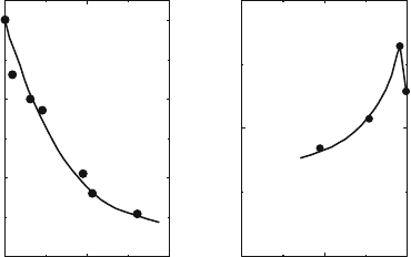
Fig. 6.5. Dependence of the dislocation velocities in Ge–Si alloys on the Si content.
(a) Ge-rich alloys at 550
◦
C. (b) Si-rich alloys at 800
◦
C. Stress τ =20MPa.Data
from [374]
totally blocked. Electrically active donor impurities like P, As, and Sb increase
the dislocation velocity in the high-stress region without changing m, but
decrease it at low stresses yielding an increase in m. The effect depends only
on the concentration, but not on the particular element. Acceptor impurities
like B influence the dislocation dynamics very little. Many models not treated
here have been developed to explain these observations.
In the Ge–Si alloys of elements of equal valency, the dislocation mobility
is reduced with respect to the pure constituents [374], as demonstrated by the
plots in Fig. 6.5, showing the dislocation velocities at fixed stress in depen-
dence on the concentration x of Si atoms. The interpretation will be given
below (Sect. 6.5) in connection with the macroscopic deformation data.
The in situ straining experiments on polycrystalline silicon [163] allowed
the quantitative determination of the activation parameters of the dislocation
mobility by observing individual moving dislocations and by measuring the
dependence of the average dislocation velocity as a function of the applied load
at a constant temperature, and on the temperature. The low stress exponent
of semiconductor materials is of advantage for carrying out such quantitative
in situ straining experiments in a TEM, as changes in the dislocation velocity
are achieved by comparatively strong changes in the specimen load. At each
temperature, the load exerted on the specimen was adjusted to achieve dislo-
cation velocities in a range suitable for video recording. The average effective
stress was measured by matching the shape of temporarily pinned disloca-
tion segments to loops calculated by the line tension model, as described in
Sect. 3.2.7 and in [101] for MgO single crystals. The loops calculated for the
most prominent slip system (111) (a/2)[10
¯
1] were plotted in the projection of
the actual video recordings onto a (
¯
112) image plane. Dislocation segments
were selected, which fitted the ellipticity of the calculated loops. The relation
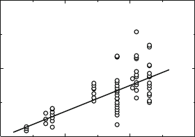
between the load and the effective stress is shown in Fig. 6.6.
216 6 Semiconductors
200
100
0
0
5
10
15
F (N)
τ
∗
(MPa)
530°C
585°C
625°C
690°C
Fig. 6.6. Dependence of the effective stress τ
∗
in polycrystalline Si on the load
applied to the in situ tensile specimen. Data from [163]
The stress exponent was determined to be m =1.6 by applying five differ-
ent loads at a constant temperature of 530
◦
C and by plotting the logarithm of
the dislocation velocities v
d
vs. the logarithm of the effective stress τ
∗
. Similar
to the X-ray topography experiments in [262], the velocities were measured on
continuously moving dislocations so that the difference between the present
value and the exponent of unity found in [262] is not due to pinning as in
the etching studies. It may result from a lower purity of the present solar
grade crystals, the pinning of the dislocations by jogs, or the effects of radi-
ation in the HVEM, as will be described later. To obtain an Arrhenius plot
of the logarithm of the dislocation velocity vs. the reciprocal temperature,
dislocation velocities measured at different temperatures and under different
loads were normalized to a constant effective stress of τ
∗
=30MPausing
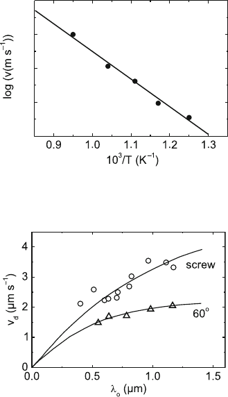
the above stress exponent and (4.103). The resulting Arrhenius plot is pre-
sented in Fig. 6.7. From the slope of this plot follows an activation energy of
ΔG
0
=(1.6 ± 0.3) eV. This energy is essentially lower than that determined
by other techniques. The dislocation velocities plotted by large open squares
in Fig. 4.42 are approximately equal to those measured by Imai and Sumino
[262] at high temperatures. At low temperatures, however, the dislocation
velocities in the in situ experiments are more than one order of magnitude
higher than in the X-ray topography experiments.
An earlier in situ study of the dislocation mobility in silicon by Louchet
[375] proved the dependence of the dislocation velocity on the length of the
gliding dislocations for short dislocation segments (<0.4 μm),asitispredicted
by the theory of the Peierls mechanism (4.47). More detailed data on this
effect shown in Fig. 6.8 were given in [376] for germanium and in [377] for the
compound semiconductor ZnS. The early in situ experiments on semiconduc-
tors are reviewed in [378]. These papers and theoretical ab-initio calculations
[379] confirm the high kink migration energy in elemental semiconductors
mentioned earlier.
6.4 Recombination-enhanced Dislocation Mobility 217
–4
–5
–6
–7
–8
Fig. 6.7. Arrhenius plot of the dislocation velocities normalized to a stress of
30 MPa. Data from [163]
Fig. 6.8. Dependence of the velocity of screw and 60
◦
dislocations in Ge single
crystals on the length of straight segments taken during in situ straining experiments
in a TEM at 430
◦
C and a stress of 40 MPa. Data from [376]
6.4 Recombination-enhanced Dislocation Mobility
The differences between the activation parameters determined in the in situ
experiments and the conventional ones may have several reasons. The Peierls
mechanism alone acts only at relatively low temperatures. At high temper-
atures, the dislocations are bowed out between high jogs. This transition
between two mechanisms is similar to that between the Peierls mechanism
and the localized obstacles described in Sect. 4.6. In the transition region,
the strain rate sensitivity decreases more strongly than the stress, which,
according to (4.11), is connected with an increase in the stress exponent m.
The nonconservative motion of the jogs results in the production of intrin-
sic point defects. Vacancy defects have been proved by positron annihilation
studies on Si and Ge crystals deformed under low-temperature high-stress con-
ditions (e.g. [380]). Subsequent annealing causes the vacancies to agglomerate
to clusters of about ten vacancies.
218 6 Semiconductors
The main reason of the high dislocation velocities at low temperatures dur-
ing the in situ experiments in the HVEM and the corresponding low value of
the activation energy (cathodo-plastic effect) is attributed to the recombina-
tion enhancement due to excess carriers [381]. The high-energy electron beam
in the HVEM excites a large number of electron–hole pairs, which recom-
bine in a nonradiative process in dislocation-related places. In principle, the
released energy can enhance both kink formation or migration. Respective
theories have been developed in [382, 383] and reviewed in [384]. Kink for-
mation is more probable since a single process of enhancement is necessary
for the creation of a double-kink, where the kinks afterwards spread over a
longer distance, while many enhancement events are necessary to support each
migration step over only one lattice distance. Recombination-enhanced dislo-
cation motion can also be stimulated by other kinds of radiation, for example,
laser irradiation.
Special experiments to study the influence of the electron beam on the
dislocation mobility were performed during the in situ straining experiments
in an HVEM on Ge and Si-5 at% Ge single crystals discussed above (Sect. 6.2)
[368]. At 566
◦
C, the average dislocation velocity in Ge increased by a factor
of about three, while the imaging electron beam current was increased by a
factor of five. Measurements of the dislocation velocities at different tempera-
tures but at a constant electron beam current yielded again drastically lower
activation energies than those experiments in which the stress pulse-double
etching method was applied without radiation [385].
6.5 Macroscopic Deformation Properties
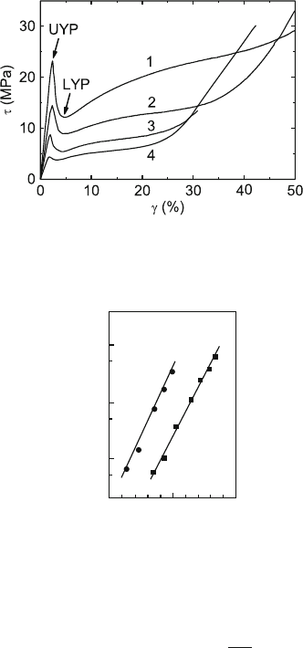
The most prominent feature of the stress–strain curves of semiconductor single
crystals oriented for single slip is the strong yield drop between the upper
(UYP) and lower yield points (LYP), as outlined in Fig. 6.9. After the lower
yield point, there follows a region of low work-hardening. The upper and
lower yield stresses show a strong dependence on the temperature, but a
weak one on the strain rate. The yield drop from the upper to the lower
yield point is a typical effect of both rapid dislocation multiplication and
the low stress exponent. At the beginning of deformation, the dislocation
density is low, leading to high dislocation velocities corresponding to a high
flow stress. With increasing dislocation density, the dislocation velocity drops
down and accordingly the flow stress, too. These features and the temperature
dependence of the flow stress of semiconductor crystals can well be modeled
by a variant of the set of constitutive equations described in Sects. 5.1.1 and
5.2 [278, 279]. Figure 6.10 presents the temperature dependence of the lower
yield stress for silicon and germanium in a plot similar to an Arrhenius plot.
The temperature and strain rate dependence of the upper and lower yield
stresses can be described by a phenomenological relation [279,359]
6.5 Macroscopic Deformation Properties 219
Fig. 6.9. Shear stress vs. shear strain curves for high-purity silicon single crystals
grown by the floating zone method and deformed along a 123 tensile axis. Strain
rate 1.2 × 10
−4
s
−1
. 800
◦
C (1), 850
◦
C (2), 900
◦
C (3), 950
◦
C (4). Data from [386]
100
10
1
0.5
1
1.5
Si
Ge
τ
ly
(MPa)
10
3
T
–1
(K
–1
)
Fig. 6.10. Temperature dependence of the lower yield stress of high-purity silicon
and germanium. Strain rate 2 × 10
−4
s
−1
. Data from [359]
τ
uy
or τ
ly
=A˙ε
1/n
exp
Q
kT
(6.1)
where A is a constant and Q is an energy.
The latter equation is not an Arrhenius relation as it does not describe
the dependence of a rate on stress and temperature. It can be derived from
the power law (4.103), which is an approximation to the Arrhenius relation
and the Orowan equation (3.5) between the strain rate and the dislocation
velocity. However, the mobile dislocation density enters the prelogarithmic
factor of the Arrhenius equation of the strain rate. As the mobile dislocation
density at the yield points strongly depends on the deformation temperature,
the prelogarithmic factor is not constant. According to [359], the correla-
tion between the microscopic activation parameters m and ΔG
0
and the
macroscopic phenomenological quantities n and Q is given by
n = m +2,Q=ΔG
0
/(m +2).
220 6 Semiconductors
The reduction of the dislocation mobility by alloying the elemental semi-
conductors with additions of equal valency, as it was discussed for the Ge–Si
alloys, also yields an increase in the macroscopic flow stress [374]. The yield
stress maximum probably occurs at the concentration x =0.5. With respect to
pure Ge, the hardening is relatively weak at low temperatures but very strong
at higher ones, resulting in an almost athermal behavior at x =0.4. For lower
concentrations, the hardening can be explained by the formation of Cottrell
atmospheres (Sect. 4.11). In the concentrated alloys, ordering phenomena may
also play some role.
6.6 Summary
In the elemental semiconductors, and in most compound semiconductors, too,
the dislocation dynamics is controlled by the double-kink mechanism over the
whole range of stress and temperature that is experimentally accessible. Then,
the character of the dislocation motion is viscous and the stress and temper-
ature dependence of the dislocation velocity can be described by the power
law (4.103), with a stress exponent m between 1 and 2. The in situ experi-
ments reveal that the dislocations are straight as expected from the Peierls
mechanism only at rest and at high stresses or low temperatures. Mostly, the
dislocations contain jogs, from cross slip of some segments as well as from cut-
ting forest dislocations. The latter may be strong obstacles to glide. In mixed
dislocations, the jogs glide along the dislocations in the direction of the Burg-
ers vector. Nevertheless, this process impedes the dislocation motion owing to
the high lattice resistance. Therefore, the dislocations bow out between the
jogs, thus contributing to the flow stress. In addition, they may form dislo-
cation debris. Further obstacles to the dislocation motion are impurities and
their agglomerates. All these processes lead to values of m higher than unity,
which is expected from the pure Peierls mechanism.
During plastic deformation, most dislocations are created in localized
sources, resulting in the concentration of slip in narrow slip bands. The tem-
perature and strain rate dependencies of the macroscopic yield stresses (upper
and lower yield stress) can also be described by a power law. The stress–
strain curves can be modeled by the set of constitutive equations introduced
in Sect. 5.2. The strong yield drop effect is due to the low stress exponents
as the strong initial increase of the dislocation density results in a similarly
strong decrease of the glide resistance. At low temperatures where the glide
resistance is high, semiconductor crystals are brittle.

7
Ceramic Single Crystals
Ceramic single crystals span a very wide range of materials from ionic crystals
like the alkali halides with ionic bonding over oxides with mixed bonding to
the carbides or nitrides with strong covalent bonding. Correspondingly, the
Peierls stress and the double-kink formation energies are very different. On
the one hand, these quantities are low in the alkali halides so that the Peierls
mechanism controls the dislocation mobility and the flow stress only at low
temperatures. On the other hand, the ceramic crystals with strong covalent
bonding become plastic only at high temperatures. Typical examples of ionic
crystals and oxides are presented in this chapter. Heuer and Mitchell recently
presented a review of the dislocation and deformation properties [387]. Struc-
tural applications of ceramic materials are mostly in the form of polycrystals.
At low temperatures, their strength is limited by the brittleness, which is con-
trolled by flaws in the polycrystalline structure acting as crack nuclei. At high
temperatures, the materials creep. The creep rates are governed partly by the
properties of the grain boundaries and partly by the plastic properties of the
crystal grains, the latter of which are discussed in this chapter. A review of
creep parameters and models of polycrystalline ceramics is given in [340].
7.1 Alkali Halides
The dislocation processes during plastic deformation of alkali halide single
crystals were extensively studied in the 1960s and 1970s. An early review of
the plastic deformation is given by Sprackling [388]. These materials are con-
sidered model substances for defect properties of other solids because of several
reasons. Atomistic calculations of the defect properties are relatively easy and
reliable, as, for example, the theoretical estimation of the Peierls stress in [132].
The interatomic potentials to be considered here are the Coulomb attrac-
tion, Born–Mayer repulsion, and Van-der-Waals potentials. High purity alkali
halide crystals can be grown so that the intrinsic deformation parameters can
