Lallart M. (ed.) Ferroelectrics - Physical Effects
Подождите немного. Документ загружается.


Localized States in Narrow-Gap Ferroelectric-Semiconductor PbSnTe:
Injection Currents, IR and THz Photosensitivity, Magnetic Field Effects
529
1981). Those levels are deep; nonetheless, there may also exist shallow levels split from the
conduction-band bottom by the Coulomb potential of the center or a system of centers in the
state (s
0
p
3
) (Volkov & Ruchaiski, 1995). As it was noted in (Volkov et al., 2002), both models
are capable of providing a reasonable explanation to the effects observed in PbSnTe:In.
Available models, however, disregard the influence the ferroelectric properties of PbSnTe
have on the photoelectric phenomena in the material, and the dark conduction and
photoconduction in it is not treated in those models with due allowance for the contribution
due to contact-injected charge carriers. The change of the slope of the temperature
dependence of current at low temperatures was most often attributed to the variation of the
energy position of the level due to indium impurities in the band gap without any
explanation given to possible reasons for this phenomenon.
The purpose of the present publication is a data analysis and a development of the concept
resting on the following basic ideas:
- transport of charge carriers in PbSnTe:In with х≈0.24-0.29 is defined by contact
injection;
- the energy gap of PbSnTe:In contains localized states acting as electron traps;
- the ferroelectric phase transition has a substantial influence on the observed electrical,
magnetic, and photoelectric properties of PbSnTe:In and, above all, on the current-
voltage characteristics of samples and on the relaxation of conduction-band electrons
injected into the material by an electric field or radiation;
- the dielectric state of PbSnTe:In at helium temperatures is related with the
compositional disorder of the material as a solid solution.
We believe that the discussion of the listed, still poorly studied points will enable a better
understanding of transport phenomena in PbSnTe:In, including the situation in magnetic
fields, and will elucidate the role of the ferroelectric phase transition in PbSnTe transport
properties.
2. Temperature dependence of conductivity and capacitance, photodielectric
effect
2.1 Experimental samples and measurement procedure
We examined PbSnTe:In films MBE-grown on BaF
2
substrates (Klimov & Shumsky, 2001a,
2003). The thickness of the films was about 1 μm, their tin content was x ≈ 0.26, and the
indium content, ≅ 3%. For measuring the current-voltage and capacitance-voltage
characteristics, special comb structures formed by two metal contacts were prepared. The
length of the gap between the contacts was 15 000 μm, and the gap width was 16 to 64 μm.
In calculating the capacitance of the structure, the parallel-plate capacitor approximation
was used; the applicability of this approximation was justified by the high value of dielectric
permittivity, ε≥400. For Hall measurements, a standard Hall bar with four potentiometric
contacts was employed. The measured sample was contained in a metal chamber that
screened it from background radiation.
As the source of radiation, two sources were used. The first source, in what follows to be
referred to as the source IR
1
, was a small-size incandescent lamp in glass bulb installed
directly in the chamber with the sample; this lamp emitted radiation with λ ≤ 2 μm that,
following absorption, caused band-to-band transitions in PbSnTe:In. The second source, to
be referred to as the source IR
2
, was a tungsten incandescent-lamp spiral mounted in an
evacuated volume with a polyethylene exit window; behind the window, a combined filter
Ferroelectrics – Physical Effects
530
was installed that allowed only radiation with quantum energies lower than the band-gap
energy of PbSnTe:In to come from the volume.
2.2 Experimental data
At low temperatures, T<20 K, at zero voltage in the measurement circuit an electric current
was registered; this current could be due to the spontaneous voltage induced in PbSnTe:In
by the ferroelectric phase transition (Herrmann & Mollmann, 1983; Nasybbulin et al., 1983;
Vinogradov & Kucherenko, 1991; Klimov & Shumsky, 2001b). The strength of the observed
current decreased in time below 10
-14
A, going beyond the measurement accuracy.
At bias voltages below 0.01 V and Т=4.2 K without illumination, no direct measurement of
sample resistance was possible because the current was too weak (<10
-14
A). The dark
resistance of the sample was therefore evaluated from the proportion between the dark
current and the current under illumination, also easily measurable at low voltages, which
could be approximated into the interval of low bias voltages. The estimate gave a value
greater than 10
14
Ohm, translating into a specific-resistance value ρ> 5⋅10
12
Ohm⋅cm (Klimov
& Shumsky, 2001a).
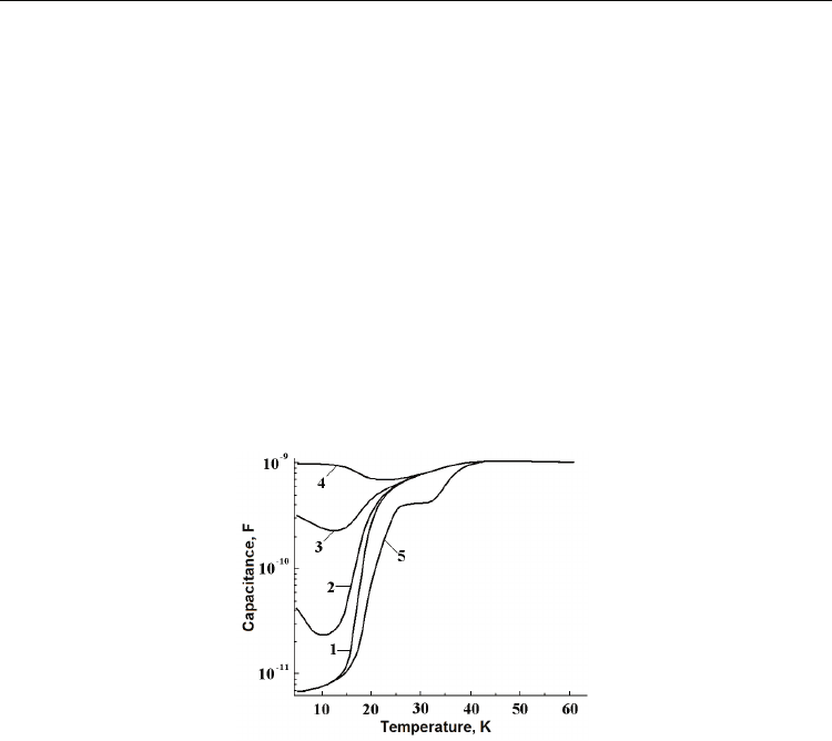
Fig. 1. The curves of sample capacitance versus temperature measured in the dark (1, 5) and
under illumination with source IR
1
(2-4). The dc bias voltages are 0 V for curves 1-4 and 1.55
V for curve 5. The voltage supplied to the source, or illumination intensity, increases on
going from curve 2 (0.14 V) to curve 4 (1.52 V), the nominal operating voltage of the source
being 6 V.
Figure 1 shows the curves of capacitance versus temperature in a sample under zero bias
voltage measured in the dark and under illumination, and also a similar curve measured in
the dark under dc bias voltage U=1.55 V at frequency f=3.3 kHz (Klimov & Shumsky, 2001a,
2003). A specific feature displayed by the curves is a decrease of capacitance reaching
approximately one hundred times on decreasing the temperature from Т=25 К to Т=15 К
without illumination, and also a weak variation of the capacitance in the same temperature
interval under illumination. In other words, illumination of the sample at temperatures
below 20 - 30 К resulted in increased capacitance of the structure. Another important feature
here is the shift towards higher temperatures of the temperature range in which the dark
capacitance exhibited strong variations on superimposing a sufficiently strong electric field
across the sample. In the latter situation, in the curve of capacitance versus temperature
there arises a characteristic shelf in the temperature interval Т=25 ÷ 30 К.
Localized States in Narrow-Gap Ferroelectric-Semiconductor PbSnTe:
Injection Currents, IR and THz Photosensitivity, Magnetic Field Effects
531
In (Vinogradov & Kucherenko, 1991) a similar temperature dependence of capacitance was
interpreted as an indication for a ferroelectric phase transition. In our samples, the
dependence of inverse dielectric permittivity on temperature has yielded for the Curie point
a value T
C
=17.5 K under zero bias voltage and a value 19.5 К under bias voltage 1.55 V.
The active and capacitive components of sample conductivity show an increase over the
temperature interval from 4.2 to 30 К both during increase of temperature under no-
illumination conditions (a) and at fixed temperature during increase of illumination
intensity (b). The relation between the concentration of free charge carriers and the sample
capacitance in both indicated situations, a and b, for the sources IR
1
and IR
2
proved to be
rather intricate.
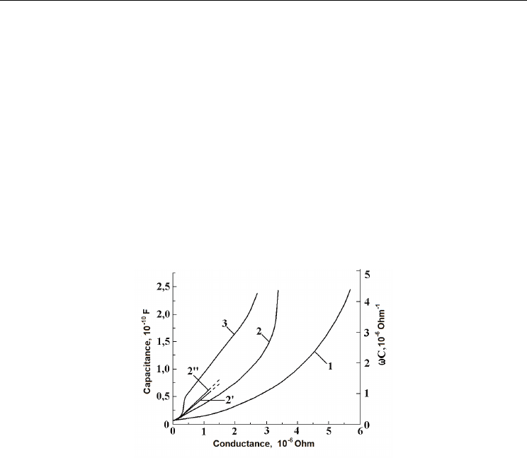
Figure 2 shows the experimental dependences of the capacitance of structure on its
conductance, C=f(σ). It could be expected that, providing that the capacitance variations
were defined by the variation of the concentration of free charge carriers in the samples,
then, no matter how the latter variation was achieved, the dependence of capacitance versus
conductivity would follow one and the same curve in the coordinates σ–C.
Fig. 2. The proportion between the active conductance of the sample R
-1
and its capacitance
(left axis) or the capacitive conductance (right axis). Frequency f=3.3 kHz. Curve 1 – growth
of conductivity and resistance due to increase of temperature from Т=4.2 К to
approximately Т=25 К. Curves 2, 2’, and 2’’ – growth of conductivity under turned-on
illumination from source IR
1
, 3 – the same with source IR
2
. The rise time of conductivity to
its maximum value: 2, 3 – 600 s, 2’ – 6 s, 2’’ – 0.4 s. The curve under illumination were
measured at Т=4.2 К.
However, the relation between the conductivity and capacitance under temperature
variations (curve 1) proved to be fundamentally different from that in illuminated sample at
liquid-helium temperature (see Figure 2). Moreover, the curve of capacitance versus
conductance in the sample illuminated with far-IR source IR
2
(curve 3) was found to show
qualitative differences from the curve displayed under illumination with source IR
1
(curves
2, 2’, 2’’). Here, although an increase in illumination intensity from source IR
1
provides for a
sharper initial growth of the curve C=f(σ), the slope of this curve tends to saturation, always
remaining several times lower than the slope of the similar curve registered with source IR
2
.
Measurements of sample capacitance versus the strength of constant electric field
superimposed onto sample performed at various temperatures under no-illumination
conditions showed that on decreasing the temperature the above dependence became less
Ferroelectrics – Physical Effects
532
pronounced (Klimov & Shumsky, 2001b). Here, in the temperature interval T < 20 K the
capacitance behaves non-monotonically as a function of electric-field strength, with an
emerging characteristic maximum whose position moves towards higher fields with
decreasing temperature.
The shape of the dependences dramatically depends on the rate of change of the electric
field (Klimov & Shumsky, 2001b). Under slowly increased field, «quenching of
photocapacitance» to the dark level is observed already under electric-field intensities of 400
V/cm. At a rapid sweep of the electric field, the dependences show an intricate behavior
with a characteristic peak displayed at E = 400 V/cm. The curves C(V) measured with
decreasing electric field differ in shape from the curves registered during an increase of the
electric field. Thus, the observed dependences with a capacitance maximum observed at a
certain electric-field strength exhibit a non-stationary dynamic pattern.
2.3 Summary
1. The current-voltage characteristics measured under illumination were linear only at
low bias voltages (< 0.015 V); the current-voltage curves measured in the dark proved
to be linear at even lower voltages.
2. At helium temperatures the films showed a spontaneous voltage typical of
ferroelectrics.
3. A photodielectric effect in PbSnTe:In films was observed. This effect consisted in a
strong (by two orders of magnitude) increase of low-frequency dielectric permittivity at
temperatures below 20 K in samples exposed to electromagnetic radiation. The effect
can be attributed to charging processes of impurity centers and to an increase of the
effective radii of those centers.
4. A more pronounced increase of capacitance (and dielectric permittivity) was observed
in samples exposed to radiation in the fundamental absorption band of PbSnTe:In.
5. The shape of measured curves of capacitance versus field strength was found to be
dependent on the rate of change of the field
Et
∂
∂ .
3. Space-charge-limited currents
3.1 Current-voltage characteristics at T=4.2 K
In «dielectric state», discussed in Introduction, at low concentrations of charge carriers in the
allowed bands transport of charge carriers should obey the theory of space-charge-limited
currents (Akimov et al., 2005). With traps for charge carriers present in PbSnTe:In, the filling
of such traps should have an influence both on the current-voltage characteristics and on the
photoconduction relaxation. Experimental structures used for measuring current-voltage
characteristics were similar to the structures described in Section 2.1. They were formed by
two metal contacts prepared on the surface of PbSnTe:In films. The length of the gap
between the contacts was 2 000 to 15 000 μm, and the gap width was 16 to 64 μm. Current-
voltage characteristics were measured in the interval of voltages up to 7-8 V using dc
sources. In measuring current-voltage characteristics at voltages in excess of 8 V, a generator
of rectangular pulses was used to avoid heating of the sample. The pulses followed at time
intervals 3⋅10
-4
s, and the width of the pulses was 1, 4, or 8 μs, depending on the voltage
range.
Figure 3 shows the current-voltage curve of an PbSnTe:In structure measured at Т=4.2 K. In
the curve, the following features are distinctly seen: a) a weak growth of the current at a
Localized States in Narrow-Gap Ferroelectric-Semiconductor PbSnTe:
Injection Currents, IR and THz Photosensitivity, Magnetic Field Effects
533
level of (2-3)
.
10
-13
A; b) voltage intervals over which the current shows first a linear and,
then, a quadratic growth; c) a transition region; and d) a quadratic dependence of the
current on voltage in the range of voltages 20 – 60 V.
Fig. 3. Current-voltage characteristics of a PbSnTe:In sample at Т = 4.2 К. The curves were
measured: (1) and (2) - under dc conditions; (3) – in pulsed mode (3).
In the region above U≈0.2 V, the current-voltage characteristics can be understood within
the theory of space-charge-limited currents (Lampert & Mark, 1970). The extended transition
region with a sharp growth of current over the voltage interval 1 to 10 V points to the
presence of various traps in the structure that at U > 20 V become filled with charge carriers.
Measurements of current-voltage characteristics at three different widths of the inter-contact
gap, 16, 32, and 64 μm, showed that, with decrease of the effective inter-contact separation
owing to metal diffusion taken into account, the experimentally measured current values
within ±10% obey the proportion
333
123 1 2 3
:: : :IIILLL
−−−
= , in line with the theory of space-
charge-limited currents.
3.2 Temperature dependence of the current
In the experimental dependences of the current on reciprocal temperature at different
voltages (see Figure 4), the following fact is engaging attention: the activation energies
Δ
E
calculated from the relation i=i
0
exp(-
Δ
E/kT) at low temperatures have different values at
different voltages: the lower the bias voltages, the lower is the activation energy.
Yet, in the temperature region T>20 K the activation energies become roughly identical for
all curves. From the standpoint of the theory of space-charge-limited currents, here we have
an increase in the concentration of equilibrium electrons, with the ohmic current dominating
the conduction. At low temperatures and not too high voltages, when the injection is still
weak, deep traps get occupied with electrons, and the activation energy determined from
the slope of i=f(10
3
/T) gives the trap energy. On increasing the bias voltage in excess of the
values at which complete filling of traps occurs (U > 3÷3.5 V) the electric current becomes
weakly dependent on temperature in the temperature region T<10÷20 K. A slight growth of
electric current with increasing temperature in this temperature region can be attributed to
variation of static dielectric permittivity in the material; this matter will be discussed in
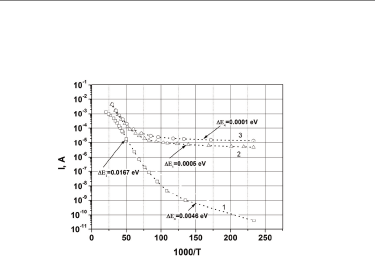
Ferroelectrics – Physical Effects
534
more detail in the next section. Note that, if the dielectric permittivity increases with
temperature, at fixed temperature it decreases with increasing the bias voltage. This
circumstance affects the observed behavior the electric current shows as a function of
temperature at the three bias voltages in Figure 4.
Fig. 4. Temperature dependence of the current through an PbSnTe:In film with х=0.25 under
bias voltages 1.55 V (1), 4.65 V (2), and 5.6 V (3). The calculated activation energies are
indicated with arrows.
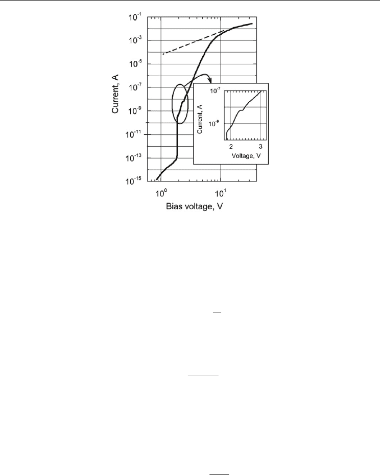
3.3 The energy distribution of traps in the forbidden band of PbSnTe:In
In (Klimov & Shumsky, 2009), current-voltage characteristics were used to extract from
them the energy distribution of traps in the forbidden band of PbSnTe:In. The current–
voltage characteristics were measured at T = 4.2 K on samples directly immersed into liquid
helium and screened from background radiation. A typical characteristic measured on one
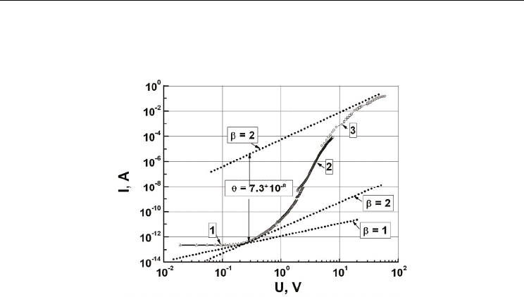
of the samples is exemplified by Fig. 5.
Following an increase of the bias voltage from 0.7 to 20 V, the electric current increases by
more than 13 orders. In a narrow range of bias voltages from 1.82 to 1.92 V the electric
current grows in value approximately by four orders. Within the theory of space-charge-
limited injection currents, this narrow range of bias voltages can be identified as a range
inside which deep traps with a discrete energy level capture electrons to finally become
completely filled with them. With further increase of bias voltage, the current grows in
value more slowly yet much faster than the quadratic dependence I~U
2
does. Such a
behavior displayed by the current–voltage curves can be attributed to a filling process in
which trap levels lying higher in energy than the above-mentioned discrete level become
filled with electrons. In the range U≥15 V, the current tends to follow the dependence I~U
2
,
which behavior corresponds to complete filling of all mentioned traps with subsequent
limitation of the electric current with the space charge induced in the material by free rather
than trapped electrons.
Localized States in Narrow-Gap Ferroelectric-Semiconductor PbSnTe:
Injection Currents, IR and THz Photosensitivity, Magnetic Field Effects
535
Fig. 5. A current–voltage characteristic measured at T= 4.2 K. Solid line—experiment,
dashed line — quadratic dependence for the current.
The energy distribution of electron traps in our samples was calculated under an
assumption that the spatial distribution of electrons in between the contacts was uniform,
this assumption being a standard one in the theory of space-charge-limited currents. In a
biased sample, for the electric current we have:
()
U
IqnUwd
L
μ
=
.
Here, μ is the electron mobility, and n(U) is the density of free electrons in the material.
From here, we readily obtain:
()
IL
nU
qwdU
μ
= .
For our sample, the effective density of conduction-band states N
c
was calculated as
described in (Anderson, 1980); at T = 4.2 K this density was found to equal N
c
≈ 4⋅10
14
cm
—3
.
The calculations showed that in the interval of bias voltages U≤10 V the density of free
electrons n(U) was smaller than N
c
and, hence, the energy position of the Fermi quasi-level
for electrons could be estimated using the simple relation
()
ln
fn c
c
nU
EEkT
N
−= .
Under conditions with space-charge-controlled limitation of the electric current, the total
charge due to free and trapped electrons is
(
)
(
)
t
QCUqnU nUwdL==⎡ + ⎤
⎣⎦
,
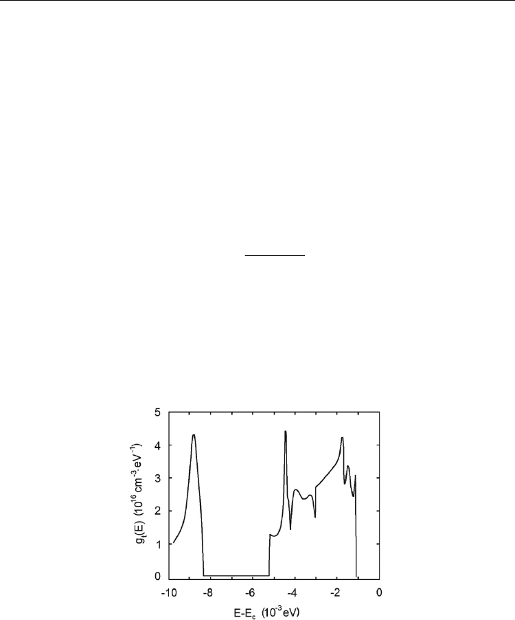
Ferroelectrics – Physical Effects
536
where C is the experimentally measured capacitance of the structure, and n
t
(U) is the
density of electrons trapped in the material. Using the values of n(U) and E
fn
(U), we can
determine, from the current–voltage curve, the dependence
()
tfn
nfE
=
. In an energy
interval between E
0
and E, the density of trapped electrons is
() ()()
0
E
tt
E
nE
g
E
f
EdE=
∫
,
where g
t
(E) is the energy distribution of traps in the material, and f(E) is the Fermi–Dirac
distribution function. Treating the Fermi–Dirac distribution function as a step function with
f(E) = 0 at energies E>E
fn
and f(E)=1 at energies E<E
fn
, we can put the upper integration limit
equal to E
fn
. After integration over E
fn
, we then obtain:
()
(
)
tfn
t
fn
nE
gE
E
⎡
⎤
∂
⎣
⎦
=
∂
.
The energy distribution of traps calculated by this formula from the experimental current–
voltage characteristic is shown in Figure 6. It should be emphasized here that the maxima
and minima distinctly observed in the trap spectrum have emerged as a result of an analysis
of an accurately measured experimental current–voltage curve. With the adopted algorithm,
trap levels below the energy level 0.01 eV from the conduction-band edge could not be
reliably identified since this could only be done by accurately measuring the current–voltage
curve in the range of currents I<10
-16
A.
Fig. 6. The energy distribution of traps extracted from measured current–voltage
characteristic.
3.4 Summary
The experimental data indicate that in PbSnTe:In samples, in which a «transition to
dielectric state» is observed, at helium temperatures the electric current remains ohmic only
in weak electric fields. On increasing the field intensity the current becomes limited by the
Localized States in Narrow-Gap Ferroelectric-Semiconductor PbSnTe:
Injection Currents, IR and THz Photosensitivity, Magnetic Field Effects
537
space charge due to electrons injected from contacts, including trapped electrons. In
structures with different separations between the contacts the current varies in inverse
proportion to the inter-electrode separation raised to the third power I~L
-3
; this finding
confirms the applicability of the theory of space-charge-limited currents to PbSnTe:In. An
analysis of the temperature dependence of the current at different bias voltages showed that
in the coordinates lgI=f(10
3
/T) the slope of the curves in the temperature range from 4.2 to 35
K strongly depends on the bias voltage. This observation can be attributed to the fact that,
on raising temperature, we have different proportions between the injected and ohmic
current. The exact value of this proportion is defined by the behavior of dielectric
permittivity as a function of temperature (the dielectric permittivity increases with
increasing temperature) and electric-field strength (the permittivity decreases with field
intensity). Thus, under conditions with space-charge-controlled limitation of the electric
current the slope of the curves lgI=f(10
3
/T) depends on the field intensity; this slope can
therefore be used for determination of trap activation energies only in weak fields. The
aforesaid also applies to interpretation of Hall data.
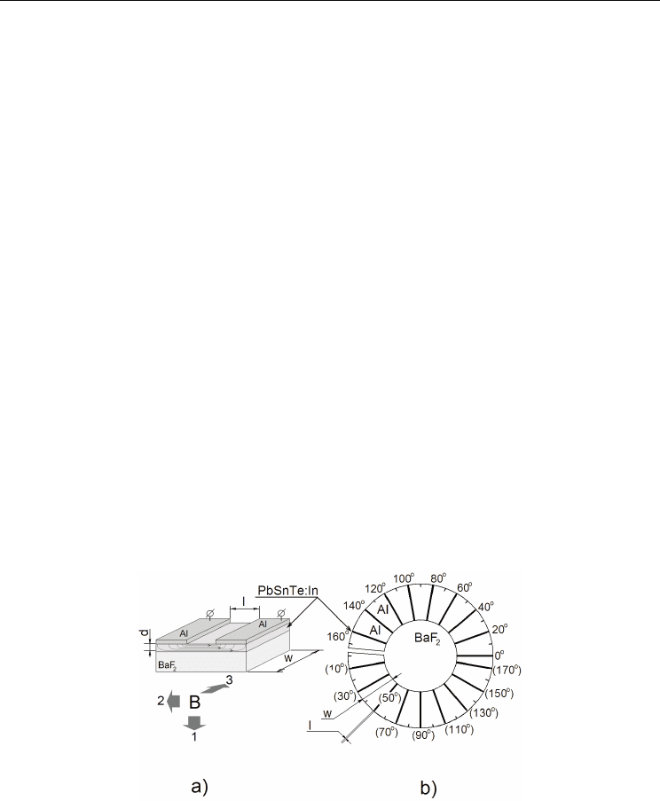
4. Transport of charge carriers in PbSnTe:In in a magnetic field
4.1 Samples
Experimental type-1 structures (S1) with metal electrodes formed on the surface of PbSnTe:In
films of thickness 1 μm were similar to the structures described in Section 2.1; these structures
are shown in Figure 7 a. Three orientations of magnetic field with respect to the electric-field
direction and the substrate-normal direction were used (Klimov et al., 2009).
The influence of gap orientation in the film plane on the current value was examined on
type-2 structures (S2), each structure comprising eighteen 0.2-cm long gaps with 30-μm
inter-electrode spacing (see Figure 7 b). In structure S2, each inter-electrode gap was turned
through angle 10° in the film plane with respect to the previous gap.
Fig. 7. Experimental structures for examining anisotropic effects in magnetic field. a) inter-
electrode gap (d=1 μm, w=0.2 cm, l=30 μm). b) arrangement of eighteen gaps on a single
crystal and their angular orientation (the «zero angle» is chosen arbitrarily).
4.2 Current anisotropy in magnetic field
Curves of relative current in magnetic field I
B
/I
B=0
versus bias voltage in an S1 structure are
shown in Figure 8 a. The current strength could be increasing or decreasing with bias
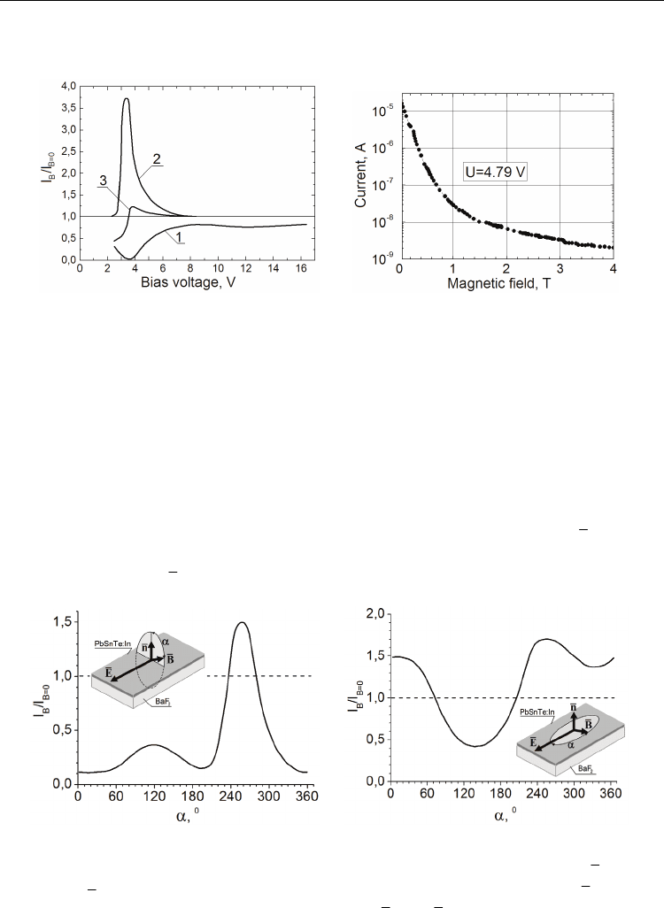
Ferroelectrics – Physical Effects
538
voltage depending on mutual orientation of the magnetic and electric fields and the normal
to the substrate. Moreover, for orientation 3 the current showed both positive and negative
(a) (b)
Fig. 8. a - Curves of relative current versus bias voltage measured at B=0.22 T. Curves 1, 2,
and 3 refer to magnetic-field vector orientations indicated in Fig. 4.1 a with the same
numerals. b - Curve of electric current versus magnetic-field strength measured at U=4.79 V.
Here, the magnetic-field vector was normal to the BaF
2
substrate.
changes with increasing bias voltage. The largest change of current was observed for
orientation 1 (Figure 7a). The relative change of current versus magnetic field for this
orientation is shown in Figure 8 b. It is seen that at B=4 T the current increases by a factor
of 10
4
.
Figure 9 shows the angular dependences of the effect at fixed bias-voltage values in
magnetic field B=0.22 T at T=4.2 K. On tuning-on and turning-off the field
B , current
relaxation over a time 10-30 sec was observed; the relaxation pattern depended on the
orientation of the field
B and on the sample temperature.
(a) (b)
Fig. 9. a - The electric current versus the angle α between the magnetic-field vector
B
and
the normal
n to the BaF
2
substrate in the plane normal to the electric-field vector
E
. b - The
electric current versus the angle α between the fields
B
and
E
in the substrate plane. The
bias voltages are U=4 V (a) and U=5 V (b).