Henini M. Handbook of Self Assembled Semiconductor Nanostructures for Novel devices in Photonics and Electronics
Подождите немного. Документ загружается.

Self-organized Quantum Dot Multilayer Structures 29
different symbols and plotted on top of each other. For the elastically isotropic case ( Fig. 1.18a ),
the dots are always vertically aligned on top of each other but there is obviously not any lateral
ordering tendency. This is revealed by the Fourier transform power spectrum of the fi nal dot posi-
tions shown in the insert. The clear discrepancy to the isotropic 1 1D growth simulations by
Tersoff et al. [17] is due to the fact that a uniform dot spacing in one dimension is not suffi cient to
produce an ordered structure in two dimensions if there is no additional in-plane anisotropy.
For the SiGe/Si (100) growth simulation ( Fig. 1.18b ), because the assumed denuded zone R
d
of 50 nm is signifi cantly larger than the lateral splitting of the energy minima induced by the
elastic anisotropy, the dots are nearly perfectly aligned in the growth direction. In addition, how-
ever, there is also a weak lateral ordering tendency along the in-plane 010 surface directions
as is indicated by the arrows in the 2D FFT power spectrum of the dot positions shown in the
upper inset of Fig. 1.18b . A detailed analysis shows that this preferred dot alignment is due to
the fact that above each dot four maxima in strain energy appear on the surface along the 011
directions away from the energy minima. This is shown by the lower inset of Fig. 1.18b , where
the strain energy distribution on the 20 nm Si spacer above a buried Ge dot is depicted over an
extended surface area and where the strain maxima are indicated by the dark colour. These
maxima cause a repulsive interlayer dot interaction and, therefore, the subsequent surface dots
tend to nucleate along the 010 surface directions relative to each other. The same result is also
found in simulations for (100) InAs/GaAs dot multilayers because the symmetry and basic shape
of the strain distribution are similar to those for the SiGe system. Due to the higher elastic anisot-
ropy, however, the observed lateral ordering tendency is even enhanced.
For the third case of (111)-oriented PbSe/PbEuTe dot superlattice growth simulations shown
in Fig. 1.18c , clearly, the lateral ordering is not only much more effi cient but also the expected
ABCABC … dot stacking is well reproduced (compare relative dot positions in the 10th, 11th and
12th layers). Even more, the lateral dot spacing in the fi nal layer of 63 nm is exactly equal to the
spacing of the surface energy minima L
3 d tan α (with d
s
50 nm and α 36 °) calculated
from the point-source model and thus reproduces very well the experimental results [18, 30, 50]
(see also section 1.6.1 for details). Figure 1.19a–d shows the evolution of the PbSe dot arrange-
ment in the simulations as a function of the superlattice period at N 1, 5, 10 and 15, respec-
tively, with the FFT power spectra of the dot positions depicted as inserts. Whereas the dots in the
initial layer are completely disordered, already after fi ve superlattice periods a clear hexagonal
lateral ordering has taken place as signifi ed by the appearance of satellite peaks in the FFT power
500
250
0
250
500
500 250 0 250 500
500
250
0
250
500
y (nm) [112]
-
-
y (nm) [112]
-
-
x (nm) [110]
-
500 250 0 250 500
x (nm) [110]
-
(a) 1st layer
(b) 5th layer
(c) 10th layer
dot size (a.u.)
Number of dots
0 200 600400
N 1
2
3
4
5
7
10
N 20
(e) Dot size distributions
(d) 15th layer
150
100
50
0
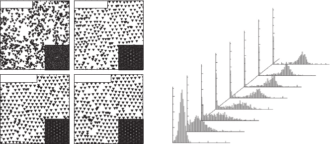
Figure 1.19 Monte Carlo simulation of self-organized (111) PbSe/PbEuTe dot superlattice growth, showing the
island positions (triangles) on the surface after the N 1st, 5th, 10th, and 15th superlattice period from (a) to
(d), respectively. The insets show the 2D Fourier power spectra of the island positions indicating the progressing
2D hexagonal in-plane ordering. Panel (e) shows the evolution of the dot size histograms as a function of number
of superlattice periods N , showing a signifi cant reduction of the relative width of the distributions after about four
superlattice periods. Adapted from Springholz et al. [49] .
CH001-I046325.indd 29CH001-I046325.indd 29 6/25/2008 12:27:28 PM6/25/2008 12:27:28 PM
30 Handbook of Self Assembled Semiconductor Nanostructures for Novel Devices in Photonics and Electronics
spectra (see inserts). With increasing number of periods, these satellite peaks become increas-
ingly more well defi ned and additional higher-order satellites appear. Thus, the hexagonal order-
ing rapidly improves.
Figure 1.19e shows the corresponding evolution of the size distribution as a function of the
number of superlattice periods. For the initial dot layer, the density and size are determined
merely by the chosen capture radius and deposited number of adatoms. With increasing number
of periods, obviously, a transition from the initially rather small dots to about a factor of two
larger dots in the multilayer stack occurs, which is caused by the reduced dot density induced by
the interlayer correlations. During the concomitant lateral ordering process, the size distribution
at fi rst signifi cantly broadens for the fi rst few superlattice layers but then rapidly narrows, indi-
cating a progressive size homogenization. After about ten layers, the relative width of the size dis-
tribution normalized to the average dot size saturates at a value of about half of that of the initial
layer. This indicates that the lateral ordering in multilayers can improve the uniformity of self-
assembled quantum dots. The observed transient broadening of the size distribution is caused
by the extensive rearrangement of the dot positions in the fi rst superlattice layers, which gives
rise to a larger variation in the dot size (see Fig. 1.19e ). This transient behaviour is in remarkable
agreement with our experimental observations described in section 1.6. Other growth simula-
tions focusing of various other aspects of ordering and correlation formation such as the infl u-
ence of the growth temperature can be found in [148–151] .
An important conclusion from the growth simulations is that there actually exist two
different ordering mechanisms in multilayer structures. The fi rst one is based on repulsive strain
fi elds from the subsurface dots, which results in an alignment of the surface dots along certain
surface directions in which the mutual dot repulsion is locally reduced. The second mechanism
is caused by the attractive strain fi elds of buried dots and is operative when the surface strain
energy distribution above each dot splits into several side minima. In the fi rst case, the dots are
still aligned along the vertical growth direction and the lateral ordering tendency is rather weak
and essentially only of short-range type. In the second case, the interlayer dot correlations are
of staggered type and the lateral ordering is more effi cient and of longer range. In both cases,
the anisotropy of the strain fi elds on the surface is a crucial prerequisite for the ordering proc-
ess, without this anisotropy no lateral ordering is found even for idealized growth simulations.
This conclusion also holds for the near-fi eld strain interactions when the dots can no longer be
approximated by point sources. Lateral ordering is counteracted by thermal disorder induced
by random surface diffusion and nucleation at other surface sites. Thus, in general the ordering
process in actual growth experiments will be more gradual and less effi cient than in the above
described growth simulations and it will also depend signifi cantly on the growth conditions.
In addition, it is noted that in the near-fi eld limit, anisotropic surface strain fi elds may also be
introduced by anisotropies in the island shapes. Thus, for higher-indexed growth orientations
and growth conditions that produce highly anisotropic dot shapes, a more effi cient lateral dot
ordering can be expected. This conclusion is also supported by recent growth experiments
[60–65, 142, 144] .
1.6 InGaAs/GaAs multilayers
Self-assembled InGaAs quantum dots have attracted great interest due to the high photolumi-
nescence effi ciency achieved in this material system [1–3]. This allows investigation of the
fundamental electronic properties of single dots or single stacks of dots using high-resolution
optical spectroscopy [12–14]. In addition, effi cient lasers (see, e.g. Refs. [1, 168–170]) and detec-
tors have been realized with this system and there are interesting possibilities for single photon
sources and quantum information processing devices. Therefore, this material system has been
investigated in great detail. In fact, the fi rst interlayer correlations in self-assembled quantum dot
multilayers were observed in InAs/GaAs dot superlattices [42, 43] , which has stimulated detailed
further investigations on this self-organization process.
CH001-I046325.indd 30CH001-I046325.indd 30 6/25/2008 12:27:30 PM6/25/2008 12:27:30 PM
Self-organized Quantum Dot Multilayer Structures 31
1.6.1 Pairing probability as a function of spacer thickness
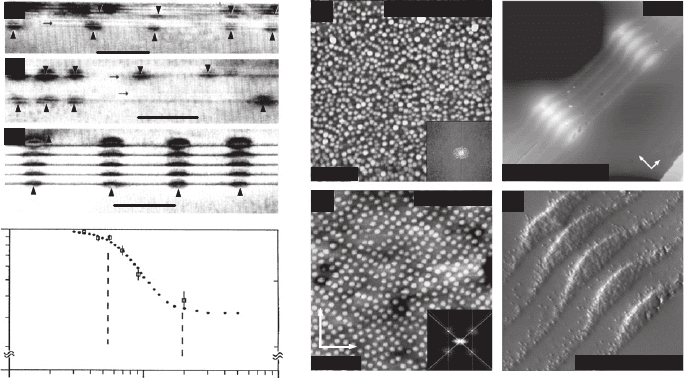
For InAs/GaAs quantum dot superlattices, it was found that the InAs dots are vertically aligned
along the (100) growth direction forming one-dimensional dot columns up to GaAs spacer thick-
nesses of around 40 nm [15, 16, 45] as shown in Fig. 1.20 . For larger spacer thicknesses, this
interlayer correlation is lost, i.e. the dots nucleate independently from those in the previous lay-
ers. This transition has been studied by Xie et al. [15] using cross-sectional transmission electron
microscopy ( Fig. 1.20a–c ) from which the pairing probability of the dots in subsequent layers
was determined as a function of spacer thickness, as shown in Fig. 1.20d . For spacer thicknesses
up to about 15 nm, the interlayer pairing probability was found to be equal to one, but then grad-
ually decreases until at about 55 nm spacer thickness no interlayer correlations were found any
more. Similar results were reported in a cross-sectional scanning tunnelling microscopy study
of Legrand et al. [45] , showing that the pairing probability depends also on the InAs dot size, i.e.
for larger dots the interlayer correlations persist to larger spacer thicknesses. In both studies, the
spacer thickness d
1/2
at which the interlayer pairing probability drops to one half was found to
be in the range of 20 to 30 nm for a growth temperature around 500°C and InAs thicknesses of
2–2.3 monolayers. This yields InAs dots with a diameter of 10 to 20 nm. For samples with dif-
ferent dot size, Legrand et al. [45] found that the crossover spacer thickness d
1/2
scales linearly
with the dot size due to the corresponding increasing strength of the strain interactions (see also
Section 1.3.4).
FFT
(e)
(g)
(f)
250 nm
FFT
250 nm
(a)
(b)
(c)
[110]
[110]
[110]
[110]
InAs single layer
30 period SL
5-fold InAs stack
XSTM
(h)
5-fold InAs stack
InAs
InAs
InAs
AlAs
_
_
50 nm
50 nm
50 nm
1
st
set islands
2
nd
set
islands
(d)
Correlated
regime
Regime with
reduced
correlation
Uncorrelated
regime
[011] cross section
1.0
0.5
0.2
Pairing probability
10 100 1000
Spacer thickness (ML)
[001]
[110]
-
Figure 1.20 Left-hand side : Cross-sectional transmission electron microscopy images of InAs/GaAs multilayers
with GaAs spacer thicknesses of (a) 42, (b) 92 and (c) 36 monolayers (ML), where for the latter the InAs dots are
perfectly aligned along the growth direction. Adapted from Xie et al. [15] . (d) Pairing probability (open squares) of
these InAs dots deduced from the transmission electron microscopy images as a function of GaAs spacer thickness.
The fi lled circles show the fi t to the experimental data using a model described in [15] . Centre : Atomic force
microscopy images of a single 3 ML InAs dot layer (e) and of a 30 period InAs/GaAs (001) dot superlattice (f)
with 6.5 nm GaAs spacers. The horizontal axis is along the [110] direction. The 2D Fourier transform (FFT) power
spectra of the topography images, shown as insets, indicate a lateral ordering of the dots along the 100 directions.
Adapted from Solomon et al. [74] . Right-hand side : Cross-sectional scanning tunnelling microscopy images of fi ve-
fold stacks of self-assembled 2.4 ML InAs dots separated by 10 nm GaAs spacer layers showing the strong changes
in dot shape and size as a function of the number of bilayers: (g) 150 1 5 0 n m
2
topography image and (f) enlarged
55 5 5 n m
2
current image. Adapted from Bruls et al. [73] .
CH001-I046325.indd 31CH001-I046325.indd 31 6/25/2008 12:27:30 PM6/25/2008 12:27:30 PM

32 Handbook of Self Assembled Semiconductor Nanostructures for Novel Devices in Photonics and Electronics
The pairing probability in the vertical dot columns was explained by Xie et al. [15] using a
model in which the lowering of the strain energy above the buried dots leads to an attraction
of mobile surface adatoms [15, 45] . The local nucleation probability was then assumed to be
proportional to the amount of accumulated InAs atoms at the strain minima. For small spacer
thickness and correspondingly deeper energy minima, all deposited adatoms within the surface
diffusion length are attracted, leading to a unity dot pairing probability. With increasing spacer
thickness, the depth of the energy minima and thus the pairing probability diminishes until the
minima become too weak to induce a correlated dot nucleation. The predictions of this model are
represented as full circles in Fig. 1.20d and were found to agree well with the experimental data
(open squares) [15, 45] . Also, a gradual transition from correlated to uncorrelated multilayers
was found in Monte Carlo superlattice growth simulations [149–151] .
1.6.2 Lateral ordering
With respect to the lateral dot ordering in (100) InAs/GaAs superlattices, Solomon et al. [74]
have shown a clear short-range dot ordering for superlattices with small GaAs spacer thicknesses
d 10 nm. As shown in Fig. 1.20f the dots are then preferentially aligned along the lateral 010
directions, whereas for the single dot reference layer no lateral order was found ( Fig. 1.20e ). This
is evidenced by the corresponding Fourier transform power spectra of the atomic force micros-
copy images shown in the inset. For the superlattice sample, four satellite peaks are seen, indi-
cating a preferred square arrangement of the dots. This is explained by Monte Carlo growth
simulations shown in Fig. 1.18 and arises from strain-induced repulsion between the buried dots
and the second nearest surface layer dots (see Section 1.5). The same type of lateral ordering was
also found by Darhuber et al. [38] for InAs dot superlattices with 20 nm GaAs spacers using high-
resolution X-ray diffraction reciprocal space mapping. Solomon et al. [31] have also reported a
signifi cant size homogenization of the dots, with a decrease of the FWHM of the dot height distri-
bution from 20% for single InAs dot reference layers to 8% in the 20 period dot superlattice.
This was also accompanied by a 25% narrowing of the photoluminescence line widths in the
superlattice to 54 meV [16, 31] . A similar narrowing was reported by Nakata et al. [75] for super-
lattices with 3 nm spacers, observing a line width decrease from 90 meV to 27 meV, and compa-
rable results were obtained by He et al. [152] . Also, for vertically aligned InP/GaInP quantum dot
superlattices a signifi cant photoluminescence narrowing from 41 to 16 meV was found [77] .
For vertically aligned (100) InGaAs/GaAs dot superlattices with In concentration of around
50% and 120 monolayer GaAs spacer thickness, another type of ordering has been recently
reported by Wang et al. [153–156] . In this case, the dots were found to be aligned in one-
dimensional dot chains along the [
011
] surface direction, as is exemplifi ed by the atomic force
microscopy image shown in Fig. 1.21a [145] . This has been attributed to the anisotropy of the
surface diffusion and the dot shapes [153–156] . The same group has also found a hexagonal
ordering when the superlattices are grown under As
2
instead of As
4
fl ux [157] .
Concerning the ordering of (100) InGaAs/GaAs multilayers with staggered dot stacking [87,
88] occurring at larger spacer thicknesses as described in Section 1.4.3, no detailed studies on
the lateral dot ordering have been reported yet. From the growth simulations and strain calcula-
tions described in the previous sections, however, it is expected that the ordering is much more
effi cient than for superlattices with vertically aligned dots. First experimental evidence that this
is really the case has been recently reported by Gutierrez et al. [88] , where a square ordering of
InGaAs dots within the growth plane was found for a staggered InGaAs/GaAs (100) multilayer
using plan-view transmission electron microscopy. A particular difference of the lateral ordering
between vertically aligned and staggered InGaAs dot superlattices is that, according to the strain
calculations and Monte Carlo growth simulations, the ordering is of short range type for the
former and of long range for the latter, as is also indicated by the experimentals [74, 88]. This
results from the fact that for vertically aligned superlattices lateral ordering is due to repulsion of
next-nearest surface dots due to the surface strain maxima induced by the buried dots along the
010 surface directions (see, e.g., inset of Fig. 1.18b ), whereas for the staggered dot stacking,
lateral ordering is caused by the square arrangement of the surface strain minima aligned along
the 010 surface directions (see, e.g., Fig. 1.9c and d ).
CH001-I046325.indd 32CH001-I046325.indd 32 6/25/2008 12:27:32 PM6/25/2008 12:27:32 PM
Self-organized Quantum Dot Multilayer Structures 33
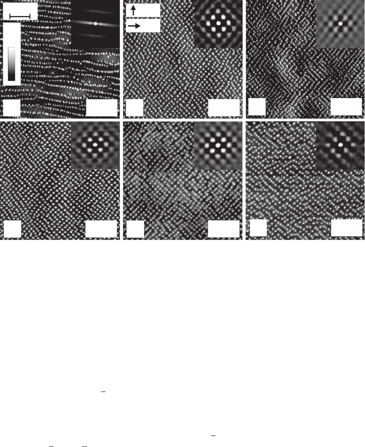
An even more effi cient 2D lateral ordering as well as an inclined interlayer dot correlation was
found by the group of Salamo et al. for InGaAs/GaAs superlattices grown on high-indexed ( n 11)B
substrates [142, 144, 145] . This is evidenced by the corresponding series of atomic force micro-
scopy images for 16.5 period superlattices on ( n 11)B substrates with n 9, 7, 5, 4 and 3 shown
in Fig. 1.21b to f , respectively, reported by Lytvyn et al. [145] . Clearly, the dots are preferentially
aligned along the in-plane
〈〉10n directions, resulting in an effi cient square ordering in the super-
lattice stack, although a faint ordering was also found for single dot layers on the high indexed
substrates [145] . The ordering was found to be best for the superlattice grown on the (411)B
orientation and was attributed to the high in-plane anisotropy of the Young’s modulus within
the growth plane with a strong minimum along the
〈〉10n
direction and pronounced maxima
along the
〈〉011
and
〈〉2nn
directions [145] . Lateral ordering of InGaAs/GaAs dots on (311)B
surfaces was also studied by Lee et al. [158] , who found only the formation of one-dimensional
dot chains on the surface. In this case, however, metal organic vapour deposition was used and
the GaAs spacer thickness was only 12 nm. On (311)B InGaAs/GaAs dot superlattices a peculiar
short-range ordering was also recently reported by Lippen et al. [159, 160] . As a consequence,
the exact ordering mechanisms are not yet resolved and remain to be investigated in detail.
1.6.3 Sizes, shapes and critical wetting layer thickness
One general feature of vertically aligned InAs dot superlattices is the signifi cant increase of the
dot size and broadening of shape along the vertical dot columns. This is illustrated in Fig. 1.20g
and h by cross-sectional scanning tunnelling images of fi ve-fold stacked 2.4 ML InAs dots sepa-
rated by 10 nm GaAs spacer layers by Bruls et al. [72, 73] . Similar changes were also found in
numerous cross-sectional scanning tunnelling [67–72] and transmission electron microscopy
[15, 16, 44] studies. From a statistical evaluation of 20 period InAs/GaAs dot superlattices,
500 nm
16
nm
(a)
100
(b) 911B
(c)
[011]
-
[2nn]
-
711B
311B
(f)
411B(e)511B(d)
Figure 1.21 Atomic force microscopy images of 16.5 period In
0.4
Ga
0.6
As/GaAs superlattices with ten monolayer
InGaAs alternating with 120 monolayer GaAs grown on (100), (911)B, (711)B, (511)B, (411)B and (311)B
substrates from (a) to (f), respectively. For the different samples on ( n 11) substrates, the horizontal direction of
the atomic force microscopy images is along [011
–
] and the vertical direction along [2
–
nn] . The insets show the 2D
autocorrelation images calculated from the atomic force microscopy images, showing the good nearly square lateral
ordering of the dots along the in-plane 1
–
n0 surface directions rotated by 45° to the horizontal [011
–
] direction.
Adapted from Lytvyn et al. [145] . The oblique interlayer correlation of dots in these samples is shown in Fig. 1.17 .
CH001-I046325.indd 33CH001-I046325.indd 33 6/25/2008 12:27:32 PM6/25/2008 12:27:32 PM
34 Handbook of Self Assembled Semiconductor Nanostructures for Novel Devices in Photonics and Electronics
Solomon et al. [31] have found a 50% increase in dot height as well as 25% increase in dot width
as compared to that of a single InAs dot reference layer. Similar changes were reported by Nakata
et al. [75] , who found in addition a signifi cant decrease of the critical wetting layer thickness for
dot nucleation from h
c
1.6 monolayers for the fi rst to 1.1 monolayers for the subsequent layers
in the multilayer stack. The latter seems to be the main reason for the substantial increase in dot
size because correspondingly more material is available for dot formation.
1.6.4 Photoluminescence
As a result of the increase in dot size, a signifi cant red shift of the photoluminescence emission of
vertically aligned InAs dots superlattice by around 100 meV has been found with respect to the
photoluminescence of single InAs dot layers [16, 31, 74, 75, 152] . The size increase should also
broaden the overall photoluminescence emission in spite of the narrowing of the size distribu-
tion in the fi nal dot layer. Therefore, contradictory results have been reported by various groups.
While on the one hand some groups have reported a signifi cant narrowing of the photolumi-
nescence emission of InAs multilayers, as mentioned above [16, 31, 75, 152, 161] , others have
found little changes [162, 163] or even a broadening of the photoluminescence emission [164–
166] . This difference may be explained also by taking the electronic coupling between the dots
into account. For very small spacer thicknesses (as applies to most experimental studies), there is
a strong overlap of the electronic wave functions of the dots in adjacent layers and thus the car-
riers are actually delocalized over several stacked dots. As a result, a certain averaging over the
vertical inhomogeneities in the dot sizes occurs. By tunnelling, the excited carriers may be trans-
ferred to the lowest energy eigenstates along the dot columns and thus a narrower photolumi-
nescence is obtained. For intermediate spacer thicknesses around 20 nm, the electronic coupling
becomes small and thus the differently red-shifted photoluminescence emission of successive dot
layers is superimposed. As a result, the emission may be signifi cantly broader as compared to that
of a single dot layer [167] , an effect that should be also strongly temperature dependent. For even
larger spacer thicknesses, the structural interaction between the dots also becomes negligible and
thus the multilayer emission will eventually approach that of a several times repeated single dot
layer [162, 163] . In spite of these complications, in most studies a notable increase in photo-
luminescence effi ciency was achieved with stacked InAs dots [16, 31, 74, 75, 152, 162, 163] .
Therefore, InAs multilayer dot structures have been successfully utilized to improve the perform-
ance of quantum dot lasers (see, e.g., [1, 4, 168–170] for reviews).
A special technique has been developed by Fafard et al. [164] to reduce the variations in dot
sizes in vertically aligned InAs multilayers. It is based on an indium fl ush step after each InAs
layer after partial capping of the dots with a thin GaAs layer. This indium fl ush step consists of
a short growth interruption during which the excess InAs that sticks out of the GaAs layer is
desorbed by a short annealing step at 610°C before continuing with superlattice growth at the
520°C growth temperature. This reduces the height of the InAs dots to the thickness of the GaAs
capping layer and the layer-to-layer dot height uniformity is signifi cantly improved [164] . As a
result, very narrow photoluminescence emission was obtained from these multilayers such that
even the s , p , and d shell structure of the electronic transitions could be observed [164] .
1.7 Ordering in SiGe/Si dot superlattices
For SiGe/Si (100) quantum dot multilayers, the general trends are quite similar as for InAs/GaAs
superlattices. From cross-sectional transmission electron microscopy [19, 32–40] as well as high
resolution X-ray diffraction [36, 38] studies, a predominant vertical alignment of SiGe dots was
found for Si spacer layers up to 50–70 nm. This is demonstrated in Fig. 1.22a by the transmis-
sion electron microscopy micrograph of a vertically aligned SiGe/Si dot superlattice with 20 nm
Si spacers grown by MBE at a temperature of 620°C [147]. The degree of interlayer correlation,
i.e. the interlayer pairing probability of Ge/Si multilayers as a function of spacer thickness, has
been studied by Kienzle et al. [35] and Stangl et al. [36] for a constant Ge thickness of 6.5 ML.
CH001-I046325.indd 34CH001-I046325.indd 34 6/25/2008 12:27:36 PM6/25/2008 12:27:36 PM
Self-organized Quantum Dot Multilayer Structures 35
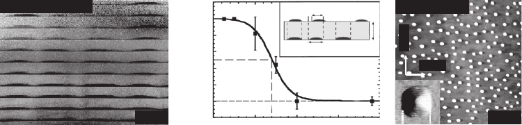
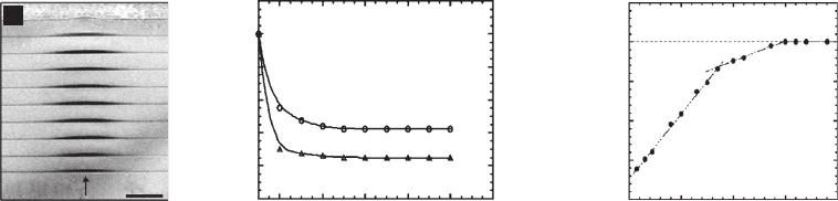
The results are shown in Fig. 1.22b , where the probability of vertical dot alignment, defi ned as
the degree of base area overlap of subsequent dots in the vertical directions as defi ned by the
inset in Fig. 1.22b , is plotted versus spacer layer thickness. For Si spacers up to 30 nm, a perfect
vertical alignment with 100% pairing probability is found. For thicker spacers the pairing proba-
bility gradually decreases until at 100 nm no interlayer correlations are formed. At 70 nm spacer
thickness, a pairing probability of 50% was found. Thus, interlayer correlations persist up to sig-
nifi cantly larger spacer thickness than for the InAs/GaAs case, which is attributed to the fact that
the Ge islands in these studies were about a factor of 5–10 times larger in diameter (85 nm) [34]
than the typical InAs dots of InAs/GaAs structures [15, 45] . In the same study, it was also found
that along the vertical Ge dot columns the dot size increases linearly with layer index number
[35] , which is most pronounced for superlattices with very thin spacers.
Apart from the changes in dot size, several studies have shown that in Si/Ge multilayers the
critical thickness for island formation decreases with increasing number of superlattice periods.
The results of a systematic UHV-CVD growth study of Le Thanh et al. [40] using in situ refl ection
high-energy electron diffraction is shown in Fig. 1.23 where the critical thickness of the 2D–3D
transition is plotted as a function of the number N of deposited Si/Ge bilayers for Si spacer thick-
nesses of 22 and 2.5 nm for a constant 4 ML thickness of the Ge layers. For the thicker Si spacers,
the critical thickness decreases by a factor of two within the fi rst four superlattice periods and
saturates thereafter at a value of about two monolayers compared to four monolayers for the fi rst
Ge layer. For the 2.5 nm thin Si spacers, the reduction is even larger, saturating at a critical thick-
ness of about 1.4 monolayers within the superlattice stack (see Fig. 1.23a ). The dependence of
the critical thickness of the second Ge layer on the Si spacer thickness is depicted in Fig. 1.23c
[40] , showing that for spacer thicknesses lower than 90 nm, the critical thickness of the second
Ge layer decreases linearly with decreasing spacer thickness, whereas for thicker spacer the criti-
cal thickness for the second Ge dot layer approaches the value of the fi rst Ge layer. This indicates
that at this point, no interlayer interactions occur any more, which agrees qualitatively with the
results of Kienzle et al. [35] displayed in Fig. 1.22b . A similar behaviour was found by Schmidt
et al. [39] for MBE grown fi ve-period Si/Ge multilayers with 25 nm thick Si spacers, where the Ge
wetting layer thickness was found to decrease from 3.8 ML for the fi rst layer to 2.5 ML in the fi fth
layer. These changes in the critical wetting layer thickness have also been shown to signifi cantly
infl uence the photoluminescence spectra from multilayer samples as is discussed in more detail,
e.g., in [22, 40] .
(a) SiGe/Si dot SL
Pairing probability
(b)
[010]
[001]
1 m
50 nm
(c) SiGe/Si SL
100 nm
Ge/Si SLs
0.0
0.2
0.4
0.6
0.8
1.0
050t
c
100
150
200
Si spacer thickness (nm)
l
i1
= 1
l
i1
= 0
L
i
B
i
t
Figure 1.22 (a) Cross-sectional transmission electron micrograph of a self-assembled (100) Si
0.5
Ge
0.5
/Si dot
superlattice showing the typical vertical alignment of the dots along the growth direction. The SiGe and Si layer
thicknesses are 2.1 and 20 nm, respectively. Adapted from Holy et al. [147]. (b) Pairing probability of 6.5 ML Ge
dots in fi ve-stack Ge/Si multilayers grown at 620°C determined by cross-sectional transmission electron microscopy
as a function of Si spacer thickness. For spacer thicknesses smaller than 40 nm, a nearly perfect dot alignment is
obtained. For larger thicknesses the pairing probability decreases such that above 100 nm, no interlayer correlations
are found. Adapted from Kienzle et al. [35] . (c) Atomic force microscopy image of the last SiGe dot layer of a 20
period SiGe/Si dot superlattice with 5.5 ML SiGe dots alternating with 30 nm Si spacers. Inset: Image of a single
SiGe dot, illustrating the typical pyramidal island shape with { 105 } side facets.
CH001-I046325.indd 35CH001-I046325.indd 35 6/25/2008 12:27:36 PM6/25/2008 12:27:36 PM
36 Handbook of Self Assembled Semiconductor Nanostructures for Novel Devices in Photonics and Electronics
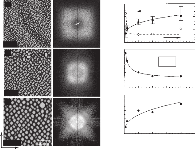
Concerning the lateral dot ordering, one has to distinguish between two different cases accord-
ing to the density and spacing of the dots in the fi rst superlattice layer that strongly depend on
the composition and thickness of the SiGe dot layers and the chosen growth conditions. For the
case of high-density SiGe hut cluster islands deposited at temperatures around 550°C, Teichert
et al. [17, 21, 28] have demonstrated a quite effective lateral ordering of SiGe hut islands along
the 100 directions, with the formation of a preferred square nearest neighbour dot arrange-
ment. This is illustrated by the atomic force microscopy images and corresponding Fourier trans-
form power spectra of Teichert et al. [21, 28] obtained for Si
0.25
Ge
0.75
/Si multilayers with N 1 ,
2 and 20 periods shown in Fig. 1.23a to c , respectively. Clearly, the lateral ordering progresses
rapidly with increasing number of deposited periods. This is accompanied by an almost three-fold
increase of the dot size but the uniformity of the dots in the fi nal dot layer signifi cantly improves.
This is demonstrated by the data displayed in Fig. 1.23d–f , where the evolution of the lateral dot
spacings, the lateral aspect ratio as well as root mean square roughness that is proportional to
the dot height are plotted versus N , respectively.
In the second case of low-density dots formed by growth of pure Ge at higher temperatures
as used in most other studies [33–36, 38–40] , the dots of single layers are already much more
uniform and widely spaced. As a result, the Ge dots in these multilayers show only a very faint
lateral ordering tendency (see Fig. 1.22c ) even at small spacer thicknesses, with only a very weak
tendency of a lateral alignment of the dots along the 100 directions, as has been found, e.g., by
X-ray diffraction studies [32, 36, 38] . These fi ndings are attributed to the weak lateral overlap of
the strain fi eld of the dots and the weak ordering tendency is in good agreement with our Monte
Carlo growth simulations [58, 147] (see section 1.5 and Fig. 1.18 ). In these simulations, the lat-
eral dot alignment along 100 as found in the experiments was explained to result from the elas-
tic anisotropy of the Si spacer material. The apparent discrepancy between the work of Teichert
et al. [21, 28] and those of the other groups [33–36, 38–40] is ascribed to the different growth
conditions, which for the former result in closely spaced dots with a large lateral strain fi eld over-
lap, whereas in the other works the lateral dot interaction is rather weak.
1.8 PbSe/PbEuTe dot superlattices
Self-assembled PbSe/PbEuTe quantum dot superlattices represent a particularly interesting sys-
tem for investigation of interlayer correlations in multilayer structures. On the one hand, the
elastic anisotropy is particularly large and, therefore, an exceedingly effi cient vertical and lateral
ordering takes place [18, 30] . On the other hand, different dot stacking types occur in dependence
of spacer thicknesses as well as growth conditions [50–56, 57] . Because in the IV–VI compounds
(a)
Critical thickness d
c
Ge/Si SLs
Number of deposited layers
2D–3D transition time (sec)
280
240
200
160
120
80
40
d
si
= 22 nm
d
si
= 2.5 nm
Critical thickness (ML)
Si spacer-layer thickness (nm)
Ge critical thickness d
c2
(ML)
0 50 100 150 200
0
1
2
3
4
5
0.66
1.33
2
2.66
3.33
4
4.66
Si sub.
[001]
50 nm
Si spacer: 22 nm
(b)
(c)
24681012
2
nd
layer d
c2
d
c1
= 4 ML
Ge/Si double layer
Figure 1.23 (a) Change of the critical thickness for Ge islanding as a function of the number of deposited layers
N in a multilayer consisting of ten periods of 4 ML Ge alternating with 22 nm ( ) or 2.5 nm ( ) Si spacer layers.
The 2D–3D transition was determined using in situ refl ection high-energy electron diffraction and the growth was
carried out using UHV-CVD at a temperature of 550°C. (b) Change of the critical thickness d
c
2
of the second Ge
layer as a function of the Si spacer thickness at a growth temperature of 600°C. The critical thickness d
c
1
4 M L o f
the fi rst Ge layer is indicated by the dashed horizontal line. Adapted from Le Thanh et al. [40] .
CH001-I046325.indd 36CH001-I046325.indd 36 6/25/2008 12:27:36 PM6/25/2008 12:27:36 PM
Self-organized Quantum Dot Multilayer Structures 37
the (111) direction is the elastically soft direction, fcc -like dot stackings are formed in (111) mul-
tilayer structures. Therefore, this system is particularly well suited for testing the theoretical pre-
dictions of superlattice growth models. In addition, extensive systematic studies on interlayer
correlation formation have been carried out in this material system.
Self-assembled PbSe dots are produced by heteroepitaxial growth on PbEuTe (111) at a criti-
cal coverage of 2.5 monolayers [130] . For the (100) growth orientation, this islanding transi-
tion is suppressed because misfi t dislocation formation sets in already at a smaller thickness of
one monolayer [134, 135] . Therefore, self-assembled quantum dots cannot be obtained in this
growth orientation. PbSe dots are under tensile strain because their lattice constant is 5.4%
smaller than that of the underlying PbEuTe buffer layers. This is in contrast to the compres-
sively strained dots present in most other studied material systems, but from an energetic point
of view this does not make any difference because the sign of strain is removed in the elastic
energy calculations. The growth properties of single PbSe dot layers have been studied in detail
by our group [130, 171] , showing that the basic behaviour is quite similar to that of other self-
assembled quantum dot systems. In particular, PbSe dots show a well-defi ned pyramidal shape
with { 100 } side facets and very narrow size distributions [130] . The size and dot density can be
readily controlled by adjusting the growth temperature or dot layer thickness [171] , with the dot
height being typically in the range of 60 to 200 Å, and the density between 1 1 0
10
2 0
10
10
c m
2
. Because of the narrow energy band gaps, PbSe dots are also of interest for fabrica-
tion of mid-infrared quantum lasers as demonstrated in our previous work [172] . Multilayer
structures are always grown on thick strain relaxed PbTe buffer layers as virtual substrates. In
the superlattice structures, the Pb
1
x
Eu
x
Te spacer layer composition is typically in the range of
x 4 to 10%. By proper adjustment of the ternary composition, strain symmetrized superlattices
SiGe/Si SLs
(d)
(f)
FFT
FFT
FFT
N 2
N 1
N 20
1.5
1.4
1.3
1.2
1.1
1.0
5
4
3
2
1
0
0 1020304050
0.0
0.5
1.0
1.5
<1> (nm)
0
150
100
50
a
b
<a/b>
SiGe terminated
Si terminated
(nm)
Number of bilayers N
(e)
(a)
(b)
(c)
Δl/l
Figure 1.24 Atomic force microscopy images (left column) and corresponding 2D power spectra (right column) of
a SiGe surface layer of Si
0.25
Ge
0.75
/Si multilayers with increasing number of multilayer periods N 1, 2 and 20
from (a) to (c), respectively (see schematic drawings on the left). The SiGe layer thickness is 2.5 nm and the Si spacer
thickness 10 nm. Panels (d) to (f) show the evolution of characteristic island parameters as a function of number
of superlattice periods N . (d) Mean island spacing l along [100] (solid line) with the error bars indicating the
width of the size distribution, and relative width Δ l / l of the distribution of island spacings (dashed line) w.
(e) Average aspect ratio of the SiGe island bases a/b (see inset). (f) Overall root mean square roughness of the
surface topography. Adapted from Teichert et al. [21, 28] .
CH001-I046325.indd 37CH001-I046325.indd 37 6/25/2008 12:27:37 PM6/25/2008 12:27:37 PM
38 Handbook of Self Assembled Semiconductor Nanostructures for Novel Devices in Photonics and Electronics
can be produced [30] in which the number of deposited bilayers is not limited by misfi t dislocation
formation.
1.8.1 Stackings as a function of spacer thickness
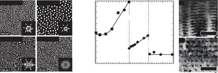
For PbSe/PbEuTe dot superlattices, the dependence of the vertical and lateral dot correlations on
spacer thickness was studied for spacer thicknesses varying from 100 to 800 Å, while the PbSe
dot layer thickness of fi ve monolayers as well as the growth conditions were kept constant. The
lateral dot ordering is illustrated in Fig. 1.25a–d , where representative atomic force microscopy
images of the fi nal dot layer after 30 superlattice periods are depicted for spacer thicknesses of
160, 320, 465 and 660 Å, respectively. In addition, the average lateral dot spacing formed in the
multilayer structure is plotted in Fig. 1.25e for a large number of samples as a function of verti-
cal superlattice period d
SL
.
[112]
300
500
700
900
1100
1300
100 200 300 400 500 600 700 800
Vertical superlattice period d
SL
(Å)
PbSe
dot SLs
(II)
Lateral dot spacing L (Å)
(I)
(III)
(d) d 660 Å(c) d 465 Å
20 nm
20 nm
(g)
d 680 Å
[110]
Vertically
aligned
ABC
stacked
D
1
c
uncor-
related
D
2
c
(f)
d 320 Å
(e)
(a) d 160 Å
(b) d 320 Å
Figure 1.25 Left-hand side : Atomic force microscopy surface images of 30 period PbSe/PbEuTe dot superlattices
with different spacer layer thickness of (a) 160, (b) 320, (c) 465 and (d) 660 Å, demonstrating the different
dot spacings and ordering tendency in the structures as evidenced by the FFT power spectra shown as insets.
(e) Preferred lateral dot spacing L plotted as a function of vertical superlattice period: squares indicate superlattices
with vertically aligned dots, diamonds those with fcc -like ABCABC … stacking and full circles those of uncorrelated
superlattices. Right-hand side : Cross-sectional transmission electron microscopy images of a vertically aligned
(f) and an uncorrelated (g) PbSe/PbEuTe dot superlattice with spacer thicknesses of 320 and 680 Å, respectively.
See Springholz et al. [50, 51] .
For spacer thicknesses lower than about 400 Å ( Fig. 1.25a and b ), there is a clear hexagonal
ordering tendency of the dots in the lateral directions [51] that is also evidenced by six peaks
in the Fourier transform power spectra of the atomic force microscopy images shown as inserts.
The lateral spacing of the dots is larger than 800 Å and rapidly increases with increasing spacer
thickness (see solid line in region I of Fig. 1.25e ). As demonstrated by the cross-sectional trans-
mission electron microscopy image of a sample with 320 Å spacer thickness shown in Fig. 1.25f ,
the dots in these samples are vertically aligned along the growth direction.
For samples with intermediate spacer thicknesses between 400 and 550 Å, the average lateral
dot spacing abruptly drops by more than a factor of two from 1300 Å to 580 Å and a very effi cient
2D hexagonal lateral ordering takes place (see Fig. 1.25c ) [18, 30, 49] . From detailed high resolu-
tion X-ray diffraction [18–20, 49, 50, 53, 55–57] as well as cross-sectional transmission electron
microscopy [19, 20, 50, 52, 54] studies already presented in Section 1.4.2, for these samples, a
well-defi ned fcc -like interlayer dot stacking (see Fig. 1.14) is formed, corresponding to an overall
trigonal three-dimensional lattice of dots as shown in Fig. 1.8a . In addition, the lateral dot spac-
ing within the superlattice stacks increases linearly with increasing spacer thickness or superlat-
tice period d
SL
, as indicated by the data and solid line depicted in region II in Fig. 1.25e . In this
range of spacer thicknesses, the interlayer correlation angle is also essentially constant at about
39° [18] , which means that the lattice constant of the resulting three-dimensional trigonal dot
lattice can be tuned over a range from 500 to 700 Å just by changes in the spacer thickness [18] .
CH001-I046325.indd 38CH001-I046325.indd 38 6/25/2008 12:27:39 PM6/25/2008 12:27:39 PM