Gibilisco S. Teach Yourself Electricity and Electronics
Подождите немного. Документ загружается.

part of this voltage passes through C
1
to the output. Because the output follows the emitter current,
this circuit is sometimes called an emitter follower circuit.
The output wave of a common collector circuit is in phase with the input wave. This circuit is
unique because its input impedance is high, while its output impedance is low. For this reason, the
common collector circuit can be used to match high impedances to low impedances. When well de-
signed, an emitter follower works over a wide range of frequencies, and is a low-cost alternative to a
broadband impedance-matching transformer.
Quiz
Refer to the text in this chapter if necessary. A good score is at least 18 correct. Answers are in the
back of the book.
1. In a PNP circuit, the collector
(a) has an arrow pointing inward.
(b) is positive with respect to the emitter.
(c) is biased at a small fraction of the base bias.
(d) is negative with respect to the emitter.
2. In many cases, a PNP transistor can be replaced with an NPN device and the circuit will do
the same thing, provided that
(a) the power supply or battery polarity is reversed.
(b) the collector and emitter leads are interchanged.
(c) the arrow is pointing inward.
(d) Forget it! A PNP transistor can never be replaced with an NPN transistor.
3. A bipolar transistor has
(a) three P-N junctions.
(b) three semiconductor layers.
(c) two N-type layers around a P-type layer.
(d) a low avalanche voltage.
4. In the dual-diode model of an NPN transistor, the emitter corresponds to
(a) the point where the cathodes are connected together.
(b) the point where the cathode of one diode is connected to the anode of the other.
(c) the point where the anodes are connected together.
(d) either of the diode cathodes.
5. The current through a transistor depends on
(a) E
C
.
(b) E
B
relative to E
C
.
(c) I
B
.
(d) more than one of the above.
Quiz 361
6. With no signal input, a bipolar transistor would have the least I
C
when
(a) the emitter is grounded.
(b) the E-B junction is forward-biased.
(c) the E-B junction is reverse-biased.
(d) the E-B current is high.
7. When a transistor is conducting as much as it can, it is said to be
(a) in a state of cutoff.
(b) in a state of saturation.
(c) in a state of reverse bias.
(d) in a state of avalanche breakdown.
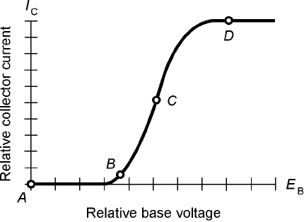
8. Refer to the curve shown in Fig. 22-12. Which operating point is best if a large amplification
factor is desired with a weak signal input?
(a) Point A
(b) Point B
(c) Point C
(d) Point D
9. In Fig. 22-12, the forward breakover point for the E-B junction is nearest to
(a) no point on this graph.
(b) point B.
(c) point C.
(d) point D.
10. In Fig. 22-12, saturation is nearest to
(a) point A.
(b) point B.
(c) point C.
(d) point D.
362 The Bipolar Transistor
22-12 Illustration for
Quiz Questions
8 through 11.
11. In Fig. 22-12, the greatest gain occurs at
(a) point A.
(b) point B.
(c) point C.
(d) point D.
12. In a common emitter circuit, the gain bandwidth product is
(a) the frequency at which the gain is 1.
(b) the frequency at which the gain is 0.707 times its value at 1 MHz.
(c) the frequency at which the gain is greatest.
(d) the difference between the frequency at which the gain is greatest, and the frequency at
which the gain is 1.
13. The bipolar-transistor configuration most often used for matching a high input impedance to
a low output impedance puts signal ground at
(a) the emitter.
(b) the base.
(c) the collector.
(d) any point; it doesn’t matter.
14. The output is in phase with the input in
(a) a common emitter circuit.
(b) a common base circuit.
(c) a common collector circuit.
(d) more than one of the above.
15. The greatest possible amplification is obtained in
(a) a common emitter circuit.
(b) a common base circuit.
(c) a common collector circuit.
(d) more than one of the above.
16. The input is applied to the collector in
(a) a common emitter circuit.
(b) a common base circuit.
(c) a common collector circuit.
(d) none of the above.
17. The configuration noted for its stability in RF power amplifiers is the
(a) common emitter circuit.
(b) common base circuit.
(c) common collector circuit.
(d) emitter follower circuit.
Quiz 363
18. In a common base circuit, the output is taken from
(a) the emitter.
(b) the base.
(c) the collector.
(d) more than one of the above.
19. Suppose that the input signal to a transistor amplifier results in saturation during part of the
cycle. This produces
(a) the greatest possible amplification.
(b) reduced efficiency.
(c) avalanche effect.
(d) nonlinear output impedance.
20. Suppose that the gain of a transistor in a common emitter circuit is 100 at a frequency of
1 kHz, and the gain is 70.7 at 335 kHz. The gain drops to 1 at 210 MHz. The alpha cutoff
frequency is
(a) 1 kHz.
(b) 335 kHz.
(c) 210 MHz.
(d) impossible to define based on this data.
364 The Bipolar Transistor
THE BIPOLAR TRANSISTOR ISN’T THE ONLY SEMICONDUCTOR TRANSISTOR THAT CAN AMPLIFY. THE
other major category of transistor is the field effect transistor (FET). There are two main types of
FET: the junction FET (JFET) and the metal-oxide FET (MOSFET).
Principle of the JFET
In a JFET, the current varies because of the effects of an electric field within the device. Charge car-
riers (electrons or holes) flow from the source (S) electrode to the drain (D) electrode. This results in
a drain current, I
D
, that is normally the same as the source current, I
S
. The rate of flow of charge
carriers—that is, the current—depends on the voltage at a control electrode called the gate (G).
Fluctuations in gate voltage, E
G
, cause changes in the current through the channel, which is the path
between the source and the drain. The current through the channel is normally equal to I
D
. Small
fluctuations in E
G
can cause large variations in I
D
. This fluctuating drain current can produce signif-
icant fluctuations in the voltage across an output resistance.
N-Channel versus P-Channel
A simplified drawing of an N-channel JFET, and its schematic symbol, are shown in Fig. 23-1. The
N-type material forms the channel, or the path for charge carriers. The majority carriers are elec-
trons. The drain is placed at a positive dc voltage with respect to the source.
In an N-channel device, the gate consists of P-type material. Another section of P-type mate-
rial, called the substrate, forms a boundary on the side of the channel opposite the gate. The voltage
on the gate produces an electric field that interferes with the flow of charge carriers through the
channel. The more negative E
G
becomes, the more the electric field chokes off the current through
the channel, and the smaller I
D
becomes.
A P-channel JFET (Fig. 23-2) has a channel of P-type semiconductor. The majority charge car-
riers are holes. The drain is negative with respect to the source. The more positive E
G
gets, the more
the electric field chokes off the current through the channel, and the smaller I
D
becomes.
365
23
CHAPTER
The Field Effect Transistor
Copyright © 2006, 2002, 1997, 1993 by The McGraw-Hill Companies, Inc. Click here for terms of use.
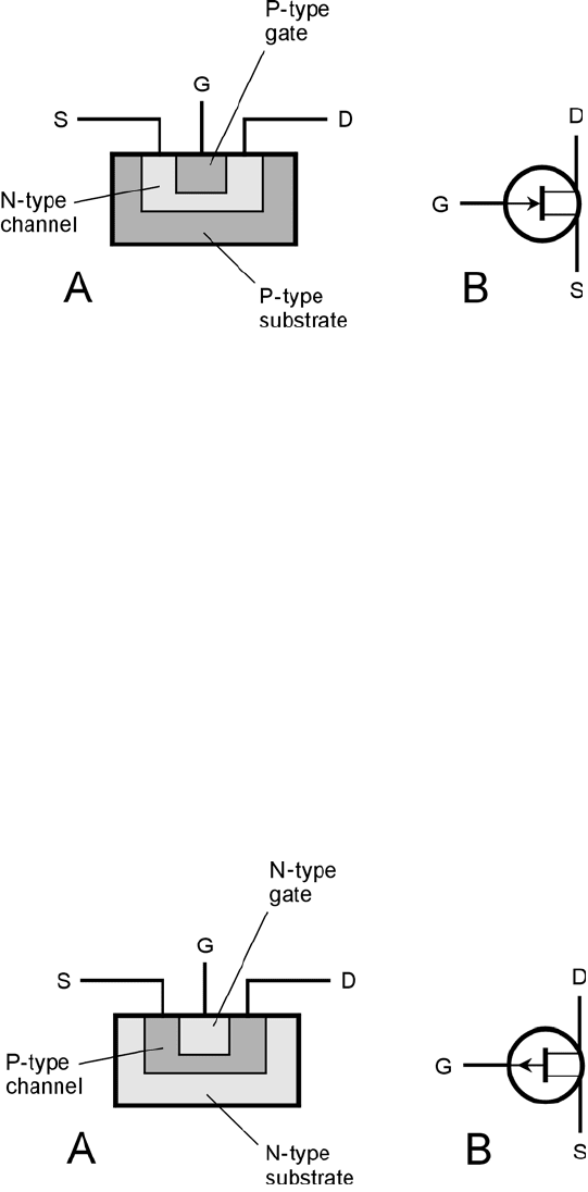
You can recognize the N-channel JFET in schematic diagrams by the arrow pointing inward at
the gate, and the P-channel JFET by the arrow pointing outward. Also, you can tell which is which
(sometimes arrows are not included in schematic diagrams) by the power-supply polarity. A positive
drain indicates an N-channel JFET, and a negative drain indicates a P-channel JFET.
In electronic circuits, N-channel and P-channel devices can do the same kinds of things. The
main difference is the polarity. An N-channel device can almost always be replaced with a P-channel
JFET, and the power-supply polarity reversed, and the circuit will still work if the new device has
the right specifications. Just as there are different kinds of bipolar transistors, there are various types
of JFETs, each suited to a particular application. Some JFETs work well as weak-signal amplifiers
and oscillators; others are made for power amplification.
Field effect transistors have certain advantages over bipolar transistors. Perhaps the most im-
portant is that FETs are available that generate less internal noise than bipolar transistors. This
makes them excellent for use as weak-signal amplifiers at very high or ultrahigh frequencies. Field
effect transistors have high input impedance, which can also be an advantage in weak-signal
amplifiers.
366 The Field Effect Transistor
23-1 At A, pictorial diagram
of an N-channel JFET.
At B, the schematic
symbol. Electrodes are
S = source, G = gate,
and D = drain.
23-2 At A, pictorial diagram
of a P-channel JFET.
At B, the schematic
symbol. Electrodes are
S = source, G = gate,
and D = drain.

Depletion and Pinchoff
The JFET works because the voltage at the gate causes an electric field that interferes, more or less,
with the flow of charge carriers along the channel. A simplified drawing of the situation for an
N-channel device is shown in Fig. 23-3.
As the drain voltage E
D
increases, so does the drain current I
D
, up to a certain level-off value.
This is true as long as the gate voltage E
G
is constant, and is not too large negatively. But as E
G
be-
comes increasingly negative (Fig. 23-3A), a depletion region (shown as a solid dark area) begins to
form in the channel. Charge carriers cannot flow in this region; they must pass through a narrowed
channel. The more negative E
G
becomes, the wider the depletion region gets, as shown in drawing
B. Ultimately, if the gate becomes negative enough, the depletion region completely obstructs the
flow of charge carriers. This condition is called pinchoff, and is illustrated at C.
JFET Biasing
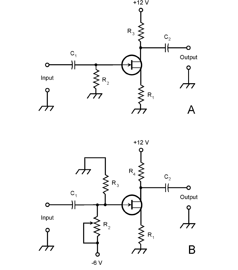
Two biasing methods for N-channel JFET circuits are shown in Fig. 23-4. In Fig. 23-4A, the
gate is grounded through resistor R
2
. The source resistor, R
1
, limits the current through the
JFET. The drain current, I
D
, flows through R
3
, producing a voltage across this resistor. The ac
output signal passes through C
2
. In Fig. 23-4B, the gate is connected through potentiometer R
2
to a voltage that is negative with respect to ground. Adjusting this potentiometer results in a
variable negative E
G
between R
2
and R
3
. Resistor R
1
limits the current through the JFET. The
drain current, I
D
, flows through R
4
, producing a voltage across it. The ac output signal passes
through C
2
.
In both of these circuits, the drain is positive relative to ground. For a P-channel JFET, reverse
the polarities in Fig. 23-4. Typical power-supply voltages in JFET circuits are comparable to those
for bipolar transistor circuits. The voltage between the source and drain, abbreviated E
D
, can range
from about 3 V to 150 V dc; most often it is 6 to 12 V dc. The biasing arrangement in Fig. 23-4A
is preferred for weak-signal amplifiers, low-level amplifiers, and oscillators. The scheme at B is more
often employed in power amplifiers having substantial input signal amplitudes.
Principle of the JFET 367
23-3 At A, the depletion region (darkest area) is narrow, the
channel (white area) is wide, and many charge carriers (heavy
dashed line) flow. At B, the depletion region is wider, the
channel is narrower, and fewer charge carriers flow. At C,
the depletion region obstructs the channel, and no charge
carriers flow.
368 The Field Effect Transistor
23-4 Two methods of biasing an N-channel JFET. At A, fixed gate
bias; at B, variable gate bias.
Amplification
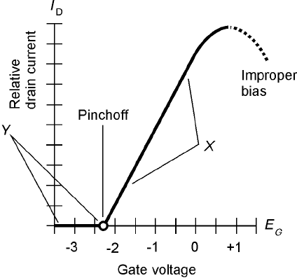
The graph of Fig. 23-5 shows I
D
as a function of E
G
for a hypothetical N-channel JFET. The drain
voltage, E
D
, is assumed to be constant. When E
G
is fairly large and negative, the JFET is pinched off,
and no current flows through the channel. As E
G
gets less negative, the channel opens up, and I
D
be-
gins flowing. As E
G
gets still less negative, the channel gets wider and I
D
increases. As E
G
approaches
the point where the S-G junction is at forward breakover, the channel conducts as well as it possi-
bly can. If E
G
becomes positive enough so the S-G junction conducts, some of the current in the
channel leaks out through the gate. This is usually an unwanted phenomenon.
The FET Amplifies Voltage
The best amplification for weak signals is obtained when E
G
is such that the slope of the curve in
Fig. 23-5 is the greatest. This is shown roughly by the range marked X. For power amplification,
however, results are often best when the JFET is biased at or beyond pinchoff, in the range
marked Y.
In either circuit shown in Fig. 23-4, I
D
passes through the drain resistor. Small fluctuations in
E
G
cause large changes in I
D
, and these variations in turn produce wide swings in the dc voltage
across R
3
(in the circuit at A) or R
4
(in the circuit at B). The ac part of this voltage goes through ca-
pacitor C
2
, and appears at the output as a signal of much greater ac voltage than that of the input
signal at the gate.
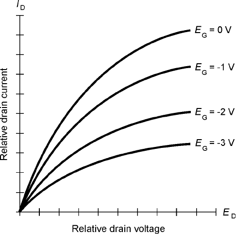
Drain Current versus Drain Voltage
Do you suspect that the current I
D
, passing through the channel of a JFET, increases in a linear man-
ner with increasing drain voltage E
D
? This seems reasonable, but it is not what usually happens. In-
stead, I
D
rises for awhile as E
D
increases steadily, and then I
D
starts to level off. The current I
D
can be
plotted graphically as a function of E
D
for various values of E
G
. When this is done, the result is a
family of characteristic curves for the JFET. The graph of Fig. 23-6 shows a family of characteristic
Amplification 369
23-5 Relative drain current
(I
D
) as a function of
gate voltage (E
G
) for
a hypothetical
N-channel JFET.
curves for a hypothetical N-channel device. The graph of I
D
versus E
G
, one example of which is
shown in Fig. 23-5, is also an important specification that engineers consider when choosing a JFET
for a particular application.
Transconductance
Recall the discussion of dynamic current amplification from the last chapter. This is a measure of how
well a bipolar transistor amplifies a signal. The JFET equivalent of this is called dynamic mutual con-
ductance or transconductance.
Refer again to Fig. 23-5. Suppose that E
G
is a certain value, resulting in a certain current I
D
. If
the gate voltage changes by a small amount dE
G
, then the drain current will change by a certain in-
crement dI
D
. The transconductance is the ratio dI
D
/dE
G
. Geometrically, this translates to the slope
of a line tangent to the curve of Fig. 23-5. The value of dI
D
/dE
G
is not the same at every point along
the curve. When the JFET is biased beyond pinchoff, in the region marked Y, the slope of the curve
is zero. Then there is no fluctuation in I
D
when E
G
changes by small amounts. There can be a change
in I
D
when there is a change in E
G
only when the channel conducts current. The region where the
transconductance, dI
D
/dE
G
, is the greatest is the region marked X, where the slope of the curve is
steepest. This region of the curve represents conditions where the most gain can be obtained from
the device.
The MOSFET
The acronym MOSFET (pronounced “moss-fet”) stands for metal-oxide-semiconductor field effect
transistor. A simplified cross-sectional drawing of an N-channel MOSFET, along with the schematic
symbol, is shown in Fig. 23-7. The P-channel device is shown in the drawings of Fig. 23-8.
370 The Field Effect Transistor
23-6 A family of
characteristic curves
for a hypothetical
N-channel JFET.
